HDI PCB vs Through-Hole PCB: Complete Comparison Guide
Printed circuit boards (PCBs) are essential platforms for connecting electronic components and enabling electrical communication within modern devices. Among various PCB technologies, HDI PCB and through-hole PCB are two representative solutions with significant differences in structure, manufacturing technology, electrical performance, cost, and application fields.
The choice between HDI PCB and through-hole PCB directly affects product size, signal performance, reliability, and manufacturing efficiency.
With the continuous development of compact and high-performance electronic products, HDI PCB technology has become increasingly important for applications requiring high-density interconnection and advanced signal performance.
1. Manufacturing Process Differences
Through-Hole PCB: Mature and Traditional Manufacturing Technology
Through-hole PCB technology is one of the most established PCB manufacturing methods.
During production, mechanical drilling equipment is used to create holes that penetrate the entire PCB structure. These holes extend from the top layer to the bottom layer.
After drilling, the hole walls are metallized through copper plating to create electrical connections between different PCB layers.
The main characteristics of through-hole PCB manufacturing include:
- Mature production technology
- Relatively simple process flow
- Lower equipment requirements
- High manufacturing stability
Because of its long development history, through-hole PCB production has become highly standardized and is widely used in applications where extreme miniaturization and ultra-high-density routing are not required.
For standard circuit board production, professional PCB Manufacturing services provide reliable and cost-effective solutions.
HDI PCB: Advanced High-Density Manufacturing Technology
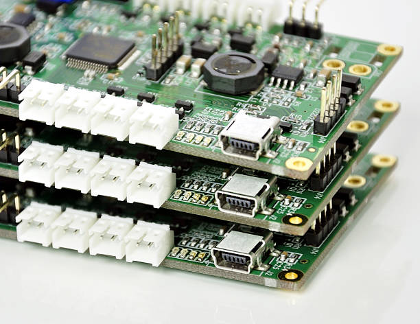
HDI PCB manufacturing uses more advanced processes, including:
- Sequential lamination
- Laser drilling
- Microvia formation
- Copper filling technology
Unlike through-hole PCBs, HDI boards use blind vias and buried vias to achieve high-density interconnections.
For example, a first-order HDI PCB usually requires:
- Layer buildup processing
- Laser drilling of microvias
- Copper plating and via filling
- Additional lamination cycles
The diameter of HDI microvias is typically much smaller than traditional drilled holes, often below 150μm.
Advanced HDI structures may include:
- Stacked vias
- Staggered vias
- Multiple buildup layers
These technologies significantly improve PCB routing density and support compact electronic designs.
For complex HDI projects requiring optimized layer structures, professional PCB Design & Layout helps engineers achieve better performance and manufacturability.
2. Via Structure Differences
Through-Hole PCB: Large Plated Through Holes
The most obvious feature of through-hole PCBs is the use of large holes that pass through the entire PCB.
These holes serve two main purposes:
- Electrical connection between PCB layers
- Mechanical mounting of through-hole components
Through-hole technology provides strong mechanical support for components, making it suitable for applications requiring high durability.
For example:
- Industrial control systems
- Power modules
- Heavy-duty electronic equipment
However, larger holes occupy more PCB space, reducing available routing area and limiting circuit density.
HDI PCB: Microvia-Based High-Density Connections
HDI PCB technology relies heavily on microvias to create compact layer connections.
Compared with traditional through holes, microvias offer:
- Smaller hole sizes
- Shorter signal paths
- Higher wiring density
- Better space utilization
The shorter electrical path helps reduce:
- Signal delay
- Transmission loss
- Parasitic effects
This makes HDI PCB technology ideal for advanced electronic products requiring miniaturization and high performance.
Professional HDI PCB manufacturing supports complex multilayer structures and high-density circuit layouts.
3. Electrical Performance Comparison
Through-Hole PCB: Reliable for Low and Medium-Speed Applications
Through-hole PCBs provide stable electrical connections and excellent mechanical reliability.
They are widely used in:
- Industrial electronics
- Control systems
- Traditional electronic equipment
However, as signal frequency increases, through holes may introduce:
- Parasitic capacitance
- Parasitic inductance
- Signal reflection
- Transmission loss
These effects can reduce signal integrity in high-speed applications.
HDI PCB: Superior Performance for High-Speed Signals
HDI PCBs provide better electrical performance because of their advanced via structures and shorter signal paths.
Advantages include:
- Improved signal integrity
- Reduced electromagnetic interference
- Better impedance control
- Lower signal transmission loss
HDI PCB technology is widely used in:
- 5G communication equipment
- High-speed servers
- Advanced computing systems
- Mobile communication devices
For products requiring high-speed signal transmission, HDI PCB provides significant advantages over traditional through-hole structures.
4. Application Differences
Through-Hole PCB Applications
Through-hole PCBs remain widely used due to their:
- High mechanical strength
- Easy maintenance
- Manufacturing reliability
- Lower cost
Typical applications include:
Industrial Equipment
Industrial control systems often operate under:
- Mechanical vibration
- Complex electromagnetic environments
- Long operating cycles
Through-hole PCBs provide stable performance in these demanding conditions.
Automotive Electronics
Many automotive electronic modules still use through-hole technology because of its mechanical durability and reliability.
HDI PCB Applications
HDI PCB is widely used in products requiring:
- Small size
- High integration
- High-speed communication
Typical applications include:
Smartphones
Modern smartphones integrate many functional modules into extremely limited space, including:
- Processors
- Communication modules
- Camera systems
- Sensors
HDI PCB enables complex routing while maintaining compact dimensions.
Consumer Electronics
HDI technology is also widely used in:
- Laptops
- Tablets
- Digital cameras
- Wearable devices
These products require lightweight structures and advanced electrical performance.
5. Cost and Maintenance Comparison
Through-Hole PCB: Lower Cost and Easier Maintenance
Through-hole PCB manufacturing uses mature processes and conventional equipment.
Advantages include:
- Lower production cost
- Simple manufacturing process
- Easy troubleshooting
- Convenient repair
Because of its straightforward structure, technicians can often identify faults using basic tools such as:
- Multimeters
- Optical inspection equipment
This makes through-hole PCB suitable for cost-sensitive applications.
HDI PCB: Higher Cost but Greater Integration Capability
HDI PCB manufacturing requires advanced equipment, including:
- Laser drilling systems
- Precision plating equipment
- High-accuracy inspection systems
The production process requires strict control of:
- Layer alignment
- Microvia reliability
- Copper filling quality
These factors increase manufacturing complexity and cost.
However, when PCB layer counts become very high, HDI technology can sometimes provide cost advantages by reducing complicated traditional lamination processes.
For prototype verification and small-volume development, Prototype PCB Assembly helps customers validate HDI designs before full-scale production.
HDI PCB vs Through-Hole PCB Comparison Table
| Comparison Item | HDI PCB | Through-Hole PCB |
|---|---|---|
| Manufacturing Technology | Laser drilling, sequential lamination | Mechanical drilling |
| Via Type | Microvias, blind vias, buried vias | Plated through holes |
| Circuit Density | Very high | Moderate |
| Signal Performance | Excellent for high-speed signals | Suitable for low and medium speeds |
| Board Size | Supports miniaturization | Requires more space |
| Manufacturing Cost | Higher | Lower |
| Mechanical Strength | Moderate | Excellent |
| Typical Applications | Smartphones, servers, 5G equipment | Industrial equipment, power electronics |
How to Choose Between HDI PCB and Through-Hole PCB?
The choice depends on product requirements.
Choose HDI PCB when the product requires:
- High-density routing
- Small form factor
- High-speed signal transmission
- Advanced electronic integration
Choose Through Hole PCB when the product requires:
- High mechanical strength
- Lower manufacturing cost
- Easy maintenance
- Large component support
Engineers should consider:
- Performance requirements
- Product size limitations
- Production volume
- Cost targets
- Long-term reliability
Conclusion
HDI PCB and through-hole PCB each have their own advantages.
Through-hole PCB remains an excellent choice for applications requiring reliability, mechanical strength, and cost efficiency.
HDI PCB represents advanced PCB technology designed for modern electronic products requiring high-density interconnections, compact structures, and superior signal performance.
As electronic devices continue moving toward smaller sizes and higher performance, HDI PCB technology will play an increasingly important role in next-generation electronics.
By selecting the right PCB structure and working with experienced PCB manufacturers, companies can achieve the optimal balance between performance, reliability, and manufacturing cost.