PCB Right-Angle Routing: Three Reasons to Avoid 90° Traces
Can PCB Traces Be Routed at 90°?
When engineers first learn PCB layout, one of the most common rules is to avoid 90° trace corners. However, PCB right-angle routing is not always prohibited. Whether it should be avoided depends largely on the electrical characteristics of the circuit, particularly its signal frequency and edge rate.
For low-frequency circuits, a 90° corner generally has little practical impact. For high-speed or RF circuits, however, right-angle routing can introduce impedance discontinuities, reflections, parasitic effects, and EMI concerns.
The following three factors explain why PCB designers generally prefer 45° or curved routing.
1. High-Frequency Signals Are Sensitive to Right-Angle Corners
The most important factor is signal frequency.
At a 90° corner, the effective trace width at the bend can become larger than the nominal trace width. This geometry change can reduce the local impedance and create an impedance discontinuity. The discontinuity may cause part of the signal to reflect back toward the source rather than continuing smoothly along the transmission line.
For low-frequency signals, these effects are usually negligible because the signal wavelength is much longer than the PCB trace length. In many low-speed designs, traces can therefore be treated approximately as lumped connections rather than transmission lines.
For high-speed signals, the situation is different. Signal edges can contain significant high-frequency components even when the clock frequency itself does not appear particularly high. As a result, trace geometry and impedance continuity become increasingly important.
Right-Angle Routing and PCB Trace Impedance
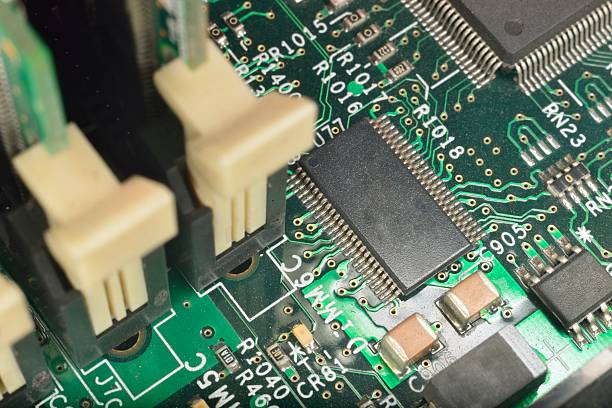
In High-Speed PCB Design, maintaining consistent trace geometry is essential for controlling PCB Trace Impedance.
For example, suppose a controlled-impedance trace is designed for a nominal impedance of 50 Ω. If the trace width at a 90° corner increases significantly, the local impedance can drop well below the target value. This discontinuity can produce signal reflections and affect waveform integrity.
For a practical high-speed design, engineers may specify an impedance tolerance such as ±10%, depending on the interface and design requirements. A 50 Ω transmission line would therefore have a target range of approximately 45–55 Ω.
The exact impedance depends on multiple parameters, including:
- Trace width
- Trace thickness
- Dielectric thickness
- Dielectric constant
- Reference plane
- Copper geometry
- Stackup configuration
This is why impedance-controlled traces should be evaluated as part of the complete PCB stackup rather than by trace width alone. GOPCBA provides professional PCB Design & Layout services to support stackup, layout, and manufacturability considerations.
Why 45° and Curved Routing Are Preferred
A curved trace maintains a more consistent geometry through the bend and therefore minimizes abrupt changes in impedance. For demanding RF applications, smooth curved routing can be preferred when minimizing discontinuities is particularly important.
In most conventional PCB layouts, however, 45° routing is the practical standard. It provides a good balance between electrical performance, routing efficiency, and manufacturability.
Therefore, the general preference is:
90° corner → Avoid when possible
45° corner → Commonly preferred
Curved corner → Best for applications requiring particularly smooth transitions
2. Right-Angle Routing Can Create PCB Manufacturing Problems
Electrical performance is not the only reason to avoid sharp corners. PCB fabrication processes also favor routing geometries that do not create unnecessarily narrow or sharp features.
During PCB etching, chemicals must flow evenly across the copper pattern. Extremely acute angles can create areas where etching chemicals become trapped, a phenomenon commonly referred to as an acid trap.
What Is an Acid Trap?
An acid trap occurs when a narrow, acute-angle region in the copper pattern retains etching solution. Because the chemical solution may not be removed evenly, localized over-etching can occur.
This can potentially reduce conductor width and, in severe cases, contribute to open circuits or other fabrication defects.
Acute-angle routing is therefore generally avoided in professional PCB layouts. Right-angle routing is less problematic than an extremely sharp acute angle, but it is still commonly discouraged when a cleaner routing geometry can be used.
This consideration becomes particularly important when designing traces connected directly to pads. The trace should leave the pad without creating an unnecessarily sharp angle or narrow copper region.
For production designs, proper layout should be reviewed together with fabrication requirements. GOPCBA’s PCB Manufacturing service integrates PCB fabrication considerations into the manufacturing process.
3. 90° Corners Are Usually Less Practical for Professional Layout
There is also a practical design reason: clean routing geometry makes PCB layouts easier to review, maintain, and manufacture.
Modern PCB layout standards generally favor 45° corners or curved transitions rather than repeated 90° bends. This approach creates cleaner routing paths and makes the board easier to inspect visually.
For large-current traces, designers may also use copper pours or wider copper regions instead of narrow traces. When the copper region changes direction, using two 45° transitions instead of a single 90° corner can provide a cleaner geometry while maintaining an orderly layout.
However, aesthetics should never override electrical or manufacturing requirements. The routing strategy should always be determined by the signal type, current level, impedance requirements, layer structure, and manufacturing capability.
When Is 90° Routing Acceptable?
It is important not to turn the rule into an absolute requirement.
A 90° corner may be acceptable when:
- The circuit operates at relatively low speed.
- Controlled impedance is not required.
- Trace lengths are electrically short.
- Signal integrity is not a critical concern.
- The manufacturing design rules permit the geometry.
- Space constraints make alternative routing impractical.
For high-speed interfaces, RF circuits, and other impedance-controlled applications, however, designers should generally avoid unnecessary 90° corners.
In these designs, Signal Integrity should be evaluated based on the complete interconnect rather than simply following a routing rule. Trace length, return-current paths, vias, reference planes, connectors, and impedance discontinuities can all affect system performance.
90° Routing vs. 45° Routing
| Routing Method | Typical Application | Main Consideration |
|---|---|---|
| 90° routing | Low-speed, non-critical signals | Usually acceptable when electrical constraints are limited |
| 45° routing | General PCB layout | Good balance of electrical performance and manufacturability |
| Curved routing | RF and demanding high-speed applications | Minimizes abrupt geometry changes |
The correct routing method should ultimately be selected according to the electrical and manufacturing requirements of the specific PCB.
For prototype development, engineers can also validate layout decisions before committing to larger production volumes. GOPCBA’s Rapid PCB Prototyping service can be used as part of a prototype-to-production workflow.
How to Avoid Problems Caused by Right-Angle Traces
When designing a PCB, engineers can follow several practical guidelines:
- Use 45° routing instead of unnecessary 90° corners.
- Use curved traces for demanding RF applications when appropriate.
- Maintain consistent trace width through bends.
- Control impedance according to the complete PCB stackup.
- Avoid acute-angle copper geometries that may create acid traps.
- Keep high-speed traces over a continuous reference plane.
- Consider return-current paths when routing high-speed signals.
- Review routing against PCB fabrication capabilities before production.
These practices are especially important for high-speed digital, RF, networking, telecommunications, and other signal-sensitive designs.
For completed boards, electrical performance should also be verified through appropriate inspection and testing rather than relying only on visual layout rules. GOPCBA offers PCBA Testing for production validation and testing requirements.
Conclusion
PCB traces are not universally forbidden from using 90° corners. For low-frequency and electrically short connections, the impact of a right-angle bend is often insignificant.
However, as signal speed increases, trace geometry becomes increasingly important. A 90° corner can introduce an impedance discontinuity and contribute to reflections, parasitic effects, and signal distortion. Acute-angle geometries can also create manufacturing concerns such as acid traps.
For this reason, professional PCB layouts generally favor 45° routing, while curved traces may be preferred for demanding RF and high-speed applications.
The key principle is simple: avoid unnecessary 90° corners, but select routing geometry according to actual electrical and manufacturing requirements rather than treating the rule as absolute.