What Is AOI Inspection in PCB Assembly?
AOI Inspection, or Automated Optical Inspection, is an important quality-control method widely used in electronics manufacturing and PCB assembly.
AOI systems use cameras to capture detailed images of a PCB assembly and compare the actual board against predefined design or inspection criteria. Depending on the equipment, AOI may use 2D imaging or 3D optical inspection technology to identify defects in solder joints, component placement, PCB pads, and other assembly features.
When the inspection system detects a deviation from the expected condition, it flags the suspected defect for further review by an operator or quality engineer.
This makes AOI an effective method for identifying assembly defects quickly and improving process consistency.
How Does Automated Optical Inspection Work?
The basic principle behind Automated Optical Inspection is to compare the actual physical condition of a PCB assembly with expected design or process information.
A typical AOI process includes several steps:
1. Image Acquisition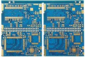
The AOI machine uses one or more high-resolution cameras to capture images of the PCB.
Depending on the inspection system, the equipment may use:
- 2D cameras
- 3D cameras
- Structured-light imaging
- Multiple viewing angles
3D AOI systems can also measure solder height, volume, and other dimensional characteristics that cannot be fully evaluated from a conventional 2D image.
2. Image Analysis
The system analyzes the captured images and compares the detected features against predefined inspection criteria.
Typical inspection targets include:
- Component presence
- Component position
- Component orientation
- Solder joint condition
- Solder paste distribution
- Pad coverage
- Polarity markings
- Missing components
- Incorrect components
3. Defect Identification
When the detected condition exceeds the defined inspection tolerance, the system marks the location for review.
An operator or engineer can then determine whether the result is:
- A genuine manufacturing defect
- A process deviation
- A false call caused by component or board characteristics
This automated inspection process allows manufacturers to identify potential defects much faster than relying entirely on manual visual inspection.
What Defects Can AOI Detect?
AOI is particularly effective for identifying visual and dimensional defects during SMT production.
Typical defects include:
- Missing components
- Misaligned components
- Incorrect component orientation
- Tombstoning
- Solder bridges
- Insufficient solder
- Excessive solder
- Solder paste misalignment
- Incorrect polarity
- Component placement errors
However, AOI is not designed to detect every possible electrical or functional problem.
This distinction is important when establishing a complete PCB Assembly Inspection strategy.
Why AOI Cannot Replace All PCB Testing Methods
AOI is a non-contact optical inspection method. It primarily evaluates what can be observed through the inspection system.
It does not normally power up the PCB and verify whether every component or circuit operates correctly.
For example, a component may appear to be correctly positioned while still having an electrical failure.
Similarly, an invisible internal defect may not be detectable through optical inspection.
Therefore, AOI should generally be used as one part of a broader inspection and testing strategy.
Common combinations include:
- AOI + Flying Probe Testing
- AOI + In-Circuit Test (ICT)
- AOI + Functional Testing
- AOI + X-ray inspection for selected applications
The appropriate combination depends on the PCB design, component package types, production volume, product complexity, and reliability requirements.
For projects requiring multiple inspection and verification methods, professional PCBA Testing can help validate the assembled board beyond visual inspection.
Where Is AOI Used in the SMT Production Process?
AOI equipment can be installed at different positions within an SMT production line.
The optimal location depends on the manufacturer’s process-control objectives.
Three common inspection points are described below.
1. AOI After Solder Paste Printing
AOI can be installed immediately after solder paste printing.
At this stage, the PCB has received solder paste but components have not yet been placed.
This makes it possible to identify printing defects before they propagate to subsequent assembly processes.
Typical Solder Paste Defects
AOI can help identify problems such as:
- Insufficient solder paste
- Excessive solder paste
- Solder paste offset
- Poor paste-to-pad alignment
- Solder paste bridging
- Missing solder paste
For example, if solder paste is printed incorrectly, the defect may later develop into a solder joint failure after component placement and reflow.
Detecting the problem immediately after printing allows engineers to correct the printing process before a large number of boards are affected.
This is particularly valuable for high-density SMT assemblies where small printing errors can have significant consequences.
2. AOI Before Reflow Soldering
Another common inspection point is after component placement but before the PCB enters the reflow oven.
At this stage, components have been placed onto the solder paste but the solder joints have not yet been formed by reflow.
This position allows the inspection system to identify defects originating from both solder paste printing and component placement.
What Can Be Detected Before Reflow?
Typical defects include:
- Missing components
- Incorrect component placement
- Component rotation
- Component offset
- Incorrect polarity
- Poor placement alignment
- Solder paste-related problems
The inspection data can also provide useful process-control information.
For example, repeated placement offsets may indicate that a pick-and-place machine requires adjustment or calibration.
This makes pre-reflow inspection useful not only for defect detection but also for monitoring SMT process stability.
For prototype and low-volume projects, integrating inspection into a controlled SMT PCB Assembly process can help identify assembly problems before they become recurring production issues.
3. AOI After Reflow Soldering
Post-reflow AOI is one of the most widely used inspection positions in SMT production.
At this stage, the soldering process has been completed, allowing the inspection system to evaluate the assembled PCB after solder joints have formed.
Why Is Post-Reflow AOI Important?
Post-reflow inspection can identify defects resulting from multiple previous process stages, including:
- Solder paste printing
- Component placement
- Reflow soldering
- Component orientation
- Solder joint formation
Typical defects may include:
- Solder bridges
- Insufficient solder
- Excessive solder
- Component misalignment
- Tombstoning
- Missing components
- Incorrect component polarity
- Poor solder joint appearance
Because post-reflow AOI evaluates the PCB after several assembly operations have been completed, it provides an important final process-control checkpoint before the board moves to subsequent inspection or testing.
AOI in Prototype and Production PCB Assembly
AOI is valuable for both prototype and production PCB assembly, although the inspection strategy may differ depending on production volume.
During prototyping, AOI can help engineers identify design-related assembly problems and validate the SMT process.
During higher-volume production, AOI provides automated, repeatable inspection that can monitor process consistency across large numbers of assembled boards.
A well-controlled PCB Assembly process can combine automated optical inspection with other quality-control procedures to improve assembly reliability.
For prototype projects, inspection is also important because correcting a process issue early can prevent the same defect from being repeated across subsequent production batches.
AOI vs. Other PCB Inspection Methods
AOI is highly effective, but it should not be considered a universal replacement for other testing technologies.
AOI
Best suited for:
- Component placement inspection
- Solder paste inspection
- Solder joint visual inspection
- Polarity verification
- Assembly process monitoring
Flying Probe Testing
Flying probe testing uses movable probes to contact test points on the PCB and verify selected electrical characteristics.
It is particularly useful for prototypes and low-volume production because it does not necessarily require a dedicated test fixture.
In-Circuit Testing
ICT evaluates electrical characteristics at designated test points and can identify certain component and circuit-level problems that cannot be detected optically.
Functional Testing
Functional testing evaluates whether the assembled PCB performs its intended function under defined operating conditions.
It can identify problems that may not be visible through AOI.
X-Ray Inspection
X-ray inspection can be useful for assemblies containing hidden solder joints or packages where critical connections cannot be adequately inspected from the surface.
For example, certain BGA solder joints are located beneath the component package and therefore cannot be directly evaluated through conventional optical inspection.
How AOI Supports PCB Quality Control
AOI provides more than simple pass/fail inspection.
Modern AOI systems can generate process data that helps manufacturers identify recurring production trends.
Engineers can analyze inspection results to determine whether defects are concentrated around:
- Specific components
- Specific PCB locations
- Specific placement machines
- Specific solder paste printing areas
- Specific production batches
This information can support preventive process adjustments.
For example, repeated component offsets may indicate a placement-machine calibration problem, while recurring solder paste defects may point to stencil alignment, printing pressure, or paste-related process issues.
The earlier these trends are identified, the easier it becomes to correct the manufacturing process.
AOI Inspection for Reliable PCBA Manufacturing
A reliable PCBA quality system should not depend on a single inspection technology.
Instead, manufacturers should combine automated inspection, electrical testing, functional verification, and process control according to the requirements of the product.
A typical quality-control flow may include:
Solder Paste Inspection → Component Placement Inspection → Pre-Reflow AOI → Reflow Soldering → Post-Reflow AOI → Electrical Testing → Functional Testing → Final Inspection
Not every project requires every step. The appropriate inspection strategy depends on the PCB design, component technologies, product application, production volume, and required reliability level.
For medical, industrial, telecommunications, energy, and other demanding applications, inspection requirements should be defined according to the product’s specific quality standards.
AOI Inspection Checklist
Before implementing AOI in a PCB assembly process, engineers and manufacturers should consider:
Design
- Are component footprints correctly defined?
- Are polarity markings clear?
- Are reference designators correctly positioned?
- Are test points available where required?
- Are critical components identified?
SMT Process
- Is solder paste printing properly controlled?
- Is component placement accurately calibrated?
- Are stencil and PCB alignment verified?
- Is the reflow profile controlled?
AOI Process
- Are inspection tolerances correctly configured?
- Are critical components assigned appropriate inspection rules?
- Are false calls monitored?
- Are recurring defects analyzed?
- Are inspection results traceable to production batches?
Final Testing
- Does AOI need to be combined with ICT?
- Is flying probe testing appropriate?
- Is functional testing required?
- Are hidden solder joints subject to X-ray inspection?
A comprehensive quality-control strategy helps ensure that visual defects, electrical problems, and functional failures are addressed through the appropriate inspection method.
Conclusion
AOI is an essential inspection technology in modern electronics manufacturing.
It uses optical imaging and automated analysis to identify component-placement, solder-paste, solder-joint, and other visible assembly defects quickly and consistently.
However, AOI Inspection cannot detect every possible electrical or functional problem. It is therefore most effective when integrated into a broader quality-control system that may include flying probe testing, ICT, functional testing, and X-ray inspection.
The ideal AOI position also depends on the production objective. Inspection after solder paste printing focuses on printing quality, pre-reflow inspection helps control placement processes, and post-reflow inspection provides comprehensive verification of the assembled PCB.
Ultimately, combining Automated Optical Inspection with appropriate electrical and functional testing provides a more complete approach to PCBA quality assurance.
For manufacturers and engineers, the goal is not simply to detect defects after they occur, but to use inspection data to continuously improve the SMT process and prevent recurring problems before they affect production quality.