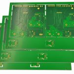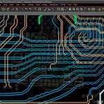
Audio quality has become an important factor in modern mobile devices. Smartphones integrate audio codecs, amplifiers, microphones, speakers, wireless communication circuits, processors, memory, displays, and power-management systems into an extremely compact space.
As a result, achieving high-quality audio is not simply a matter of selecting a better audio codec or amplifier. The PCB itself can have a significant influence on noise, distortion, crosstalk, electromagnetic interference, and overall audio performance.
A carefully engineered Mobile Phone PCB should separate sensitive audio circuits from noisy digital, RF, and power circuits while maintaining controlled return-current paths and stable power delivery.
The following design practices can help engineers improve audio performance in mobile electronic systems.
1. Plan the PCB Architecture Before Routing
Good audio performance starts with proper functional partitioning.
Before detailed routing begins, designers should divide the board into logical functional areas, such as:
- Analog audio circuits
- Digital processing circuits
- RF circuits
- Power-management circuits
- High-speed interfaces
- Clock-generation circuits
- Speaker amplifier circuits
Sensitive analog audio circuitry should be located away from major noise sources such as switching regulators, high-speed processors, memory interfaces, and RF transmitters.
The objective is not simply to create physical zones but to control how noise and return currents move through the board.
A well-planned PCB Layout can reduce unwanted coupling and make subsequent routing and debugging considerably easier.
2. Use Differential Signaling Where Appropriate
Differential signaling is widely used in high-performance audio systems because it can provide strong immunity to common-mode noise.
A differential pair carries complementary signals, allowing the receiver to reject noise that is coupled similarly into both conductors.
However, differential routing only provides these benefits when the pair is properly designed.
Important considerations include:
- Maintain consistent pair geometry.
- Keep the two traces reasonably close together.
- Control differential impedance when required by the interface.
- Minimize unnecessary discontinuities.
- Maintain a suitable reference plane.
- Avoid unnecessary vias and layer transitions.
- Match the pair length where the interface requires it.
The two conductors should generally be routed as a coupled pair rather than being separated by a ground trace.
Adding a ground trace between the two differential conductors can change their electromagnetic coupling and therefore alter the intended differential impedance. It is usually more effective to maintain appropriate pair spacing and provide a continuous reference structure beneath the pair.
For a modern Audio PCB Design, differential routing should be considered together with the complete signal path, including the codec, amplifier, connector, flex cable, speaker, and receiver circuitry.
3. Control Grounding and Return-Current Paths
Grounding is one of the most important factors affecting audio performance.
Digital circuits can generate rapidly changing currents that produce voltage fluctuations across shared impedance. If these disturbances enter sensitive analog ground structures, they may appear as audible noise.
For this reason, Grounding Design should focus on controlling return-current paths rather than simply dividing the ground plane into isolated sections.
A practical approach is to:
- Keep sensitive analog circuits physically separated from noisy digital circuits.
- Provide low-impedance return paths.
- Avoid routing sensitive signals across discontinuities in the reference plane.
- Minimize shared return paths between noisy and sensitive circuits.
- Place audio components close to their associated interfaces.
- Carefully manage connections between analog and digital ground domains.
In some designs, a carefully controlled analog/digital ground partition may be appropriate. In others, a continuous ground plane with functional placement and routing control can provide better performance.
The correct strategy depends on the device architecture and current-return behavior.
4. Minimize Audio Trace Length
Analog audio signals can be relatively sensitive to interference because their signal amplitudes may be much lower than those of digital switching signals.
Long traces increase the opportunity for coupling from:
- Digital clocks
- Processor interfaces
- Switching regulators
- RF circuits
- High-current power paths
- Display interfaces
Therefore, sensitive analog audio traces should generally be kept short and routed through electrically quiet areas.
If a longer connection is unavoidable, designers should consider shielding, differential signaling, appropriate reference planes, and controlled routing geometry.
For Mobile Phone PCB designs, physical placement is especially important because available board area is extremely limited.
5. Keep RF and Audio Circuits Properly Isolated
RF circuits are not necessarily “analog audio circuits,” even though both involve analog electrical behavior.
Mobile devices contain high-frequency RF transmitters and receivers that can generate strong electromagnetic fields and rapidly changing signals.
If RF energy couples into an audio path, nonlinearities in analog components can potentially demodulate that energy and produce audible interference.
Possible symptoms include:
- Buzzing
- Clicking
- Hissing
- Periodic interference
- GSM/LTE/5G-related noise
- Background tones associated with switching activity
To reduce this risk, designers should:
- Keep RF and sensitive audio paths physically separated.
- Use appropriate ground structures.
- Minimize exposed high-impedance audio nodes.
- Avoid routing sensitive audio traces near RF transmission paths.
- Use shielding where required.
- Carefully control connector and flex-cable transitions.
EMI Control should therefore be considered during the initial placement stage rather than treated as a troubleshooting step after PCB fabrication.
6. Do Not Mix Noisy and Sensitive Circuits Without a Clear Strategy
A common PCB design mistake is placing sensitive analog circuits too close to noisy digital or power circuitry simply because the components fit physically.
For example, an audio codec placed immediately beside a switching regulator may experience conducted or radiated noise through power, ground, or parasitic coupling.
Similarly, routing an audio signal parallel to a high-speed clock for a long distance can introduce unwanted crosstalk.
A good Mixed-Signal PCB layout should therefore consider both physical separation and electrical connectivity.
The following circuits typically deserve particular attention:
- Audio codec inputs and outputs
- Microphone paths
- Speaker amplifier inputs
- Analog reference nodes
- High-impedance sensor signals
- Clock inputs
- RF-sensitive nodes
7. Optimize Power Integrity for Audio Circuits
Power supply quality can directly affect audio performance.
Audio amplifiers, codecs, DACs, ADCs, and analog front-end circuits may be sensitive to supply ripple and transient disturbances.
This makes Power Integrity an important part of audio PCB design.
Potential noise sources include:
- Switching regulators
- DC-DC converters
- Processor load transients
- Display power circuits
- RF transmit bursts
- Battery-management circuits
Designers should consider separate filtering or regulation for particularly sensitive analog power rails when justified by the system architecture.
Low-noise LDOs, ferrite beads, LC filters, and local decoupling may be useful depending on the circuit.
However, filters should not be added indiscriminately. Their impedance, resonance, load conditions, and interaction with the regulator must be evaluated.
8. Place Bypass Capacitors Close to Power Pins
Decoupling capacitors should be placed as close as practical to the power pins they serve.
The purpose is to provide a low-impedance local current path for transient current and reduce the impact of power-distribution inductance.
For audio devices, designers should pay particular attention to:
- Codec power pins
- Analog supply pins
- Digital supply pins
- Amplifier supply pins
- Reference-voltage circuits
- PLL or clock-related supply pins
The capacitor’s effectiveness depends not only on its nominal capacitance but also on package size, ESL, ESR, via inductance, trace geometry, and placement.
A capacitor located several centimeters away from the device may provide much less effective high-frequency decoupling than a properly placed local capacitor.
9. Keep Digital Return Currents Away From Sensitive Audio Paths
Fast digital signals generate rapidly changing return currents.
At high frequencies, return current tends to follow the path of lowest impedance, which is often closely associated with the reference plane beneath the signal trace.
If a high-speed digital signal crosses a plane split or forces its return current to take a longer path, the resulting increase in loop area can increase electromagnetic coupling.
For this reason, high-speed digital traces should not be routed across gaps in their reference plane.
Sensitive audio traces should also be kept away from areas with large switching-current loops.
This approach improves both Signal Integrity and audio noise performance.
10. Use Ground Copper Carefully
Ground copper can be useful for reducing exposed signal areas and providing a low-impedance reference structure.
However, simply filling every unused PCB area with copper does not automatically improve audio performance.
Ground copper should be connected appropriately to the main ground structure and designed so that it does not create unexpected current loops or isolated floating regions.
For sensitive audio circuits, designers should verify:
- Ground-plane continuity
- Via stitching
- Return-current paths
- Analog/digital interface points
- RF shielding structures
- High-current ground paths
The objective is a predictable grounding system rather than maximum copper coverage.
11. Control Clock and Switching Noise
Audio codecs and digital audio systems can be sensitive to clock-related interference.
High-speed clock traces should therefore be routed carefully and kept away from sensitive analog inputs and outputs.
Switching regulators also deserve special attention because their high di/dt current loops can generate both conducted and radiated noise.
The following areas should be minimized where practical:
- Switching-node copper area
- High-current loop area
- Long clock traces near audio circuits
- Parallel routing between clocks and audio signals
- Shared power paths between noisy and sensitive circuits
Reducing these coupling mechanisms can significantly improve the noise floor of the audio system.
12. Pay Attention to Microphone and Speaker Paths
Microphone circuits can contain particularly low-level signals and are therefore vulnerable to external interference.
The microphone path should be kept short and protected from:
- RF transmitters
- Display interfaces
- Switching regulators
- High-speed clocks
- Speaker amplifier outputs
Speaker amplifier outputs, on the other hand, may carry substantially larger currents.
Their return paths should be designed so that high-current switching activity does not contaminate sensitive analog ground structures.
Physical separation between microphone inputs and speaker amplifier outputs can also help reduce unwanted feedback and coupling.
13. Consider Audio Performance at the System Level
PCB layout is only one part of the overall audio system.
Audio performance can also be influenced by:
- Codec architecture
- Amplifier characteristics
- Speaker impedance
- Microphone sensitivity
- Power supply noise
- Grounding
- Mechanical structure
- Acoustic chamber design
- RF activity
- Software and DSP processing
Therefore, PCB engineers should work with system and acoustic engineers when developing high-performance mobile devices.
A good PCB cannot compensate for every weakness elsewhere in the system, but poor PCB design can easily degrade an otherwise capable audio architecture.
14. Verify Audio PCB Performance Through Testing
Simulation and laboratory measurement should be used together.
Depending on the application, engineers may evaluate:
- Signal-to-noise ratio (SNR)
- Total harmonic distortion (THD)
- THD+N
- Frequency response
- Crosstalk
- Output noise
- Power-supply ripple
- Clock jitter
- EMI susceptibility
- RF desense behavior
Measurements should be performed under realistic operating conditions.
For example, the audio system should be evaluated while processors are active, displays are operating, wireless communication is transmitting, and power-management circuits are switching.
This helps identify noise mechanisms that may not appear when the audio system is tested in isolation.
15. Recommended Audio PCB Layout Checklist
Before finalizing a PCB Layout, designers can review the following points:
- Separate sensitive audio circuits from major digital, RF, and power noise sources.
- Keep sensitive analog traces short.
- Use differential signaling where appropriate.
- Maintain appropriate differential-pair geometry.
- Provide predictable return-current paths.
- Avoid routing signals across reference-plane discontinuities.
- Minimize unnecessary vias and layer transitions.
- Place bypass capacitors close to their power pins.
- Control switching-regulator current loops.
- Keep clocks away from sensitive audio paths.
- Avoid long parallel routing between noisy and sensitive traces.
- Optimize analog and digital power distribution.
- Evaluate RF-to-audio coupling.
- Verify grounding and shielding structures.
- Perform system-level audio and EMI testing.
16. Kingda’s Approach to Audio-Focused PCB Manufacturing
High-quality audio performance requires not only good circuit design but also consistent PCB manufacturing.
Variations in layer registration, dielectric thickness, copper geometry, via structures, grounding structures, and surface conditions can affect the electrical behavior of a PCB.
For compact mobile devices, manufacturing accuracy becomes especially important because high-density routing leaves less margin for process variation.
Kingda can support customers with PCB manufacturing requirements involving:
- High-density multilayer PCBs
- Fine-line routing
- Controlled impedance
- HDI structures
- High-speed signal routing
- RF and mixed-signal PCB designs
- Precision via structures
- Reliable PCB fabrication and testing
By considering PCB design, material selection, manufacturing tolerances, and assembly requirements together, engineers can achieve a more consistent and reliable audio platform.
Conclusion
Improving smartphone audio performance requires more than selecting high-performance audio components. The Mobile Phone PCB must be designed to control noise, return currents, power fluctuations, electromagnetic coupling, and signal integrity within a highly integrated electronic environment.
Effective Audio PCB Design should combine careful functional partitioning, appropriate differential routing, controlled Grounding Design, optimized Power Integrity, and effective EMI Control.
At the same time, a well-engineered Mixed-Signal PCB should ensure that sensitive audio circuits remain protected from high-speed digital, RF, and switching-power noise.
By addressing these factors from the early design stage and validating the finished PCB through system-level testing, manufacturers can achieve cleaner audio signals, lower noise, better reliability, and more consistent product performance.
Kingda provides PCB manufacturing solutions for high-density, high-speed, RF, and mixed-signal applications, helping customers turn demanding electrical and audio requirements into manufacturable PCB designs.