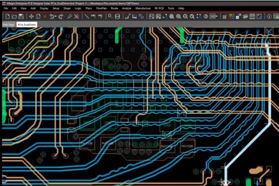
Cadence is a widely used electronic design automation (EDA) platform that supports many stages of electronic product development, including ASIC design, FPGA development, and printed circuit board design. For complex and high-speed electronic products, Cadence PCB Design provides an integrated environment for schematic capture, component and footprint development, PCB layout, routing, constraint management, simulation, and manufacturing preparation.
As PCB designs become increasingly dense and operating frequencies continue to rise, traditional layout methods are often insufficient for controlling signal integrity, power integrity, timing, crosstalk, and electromagnetic compatibility. A constraint-driven design methodology can help engineers identify potential problems earlier and reduce costly design iterations.
Cadence PCB Design Methodology
Modern high-speed PCB projects increasingly adopt a constraint-driven and simulation-assisted approach to shorten development cycles and improve design quality.
The first step is to establish a set of physical and electrical design rules based on the required system performance. These rules can then be applied to control PCB Layout and PCB Routing throughout the design process.
Rather than waiting until the physical board has been completed, engineers can perform preliminary simulations before final component placement and routing. This allows different design options to be compared virtually and helps identify potential problems before they become manufacturing issues.
Typical design constraints may include:
- Trace width and spacing
- Controlled impedance requirements
- Differential-pair parameters
- Maximum routing length
- Propagation delay
- Via structures and via counts
- Layer assignments
- Crosstalk limits
- Return-current paths
- Power distribution requirements
- Electromagnetic compatibility requirements
Establishing these constraints at an early stage creates a clear relationship between system-level performance requirements and physical PCB implementation.
Simulation-Assisted High-Speed PCB Design
Simulation is particularly important for high-speed electronic products because signal behavior is affected by more than just the schematic.
Factors such as dielectric constant, dielectric thickness, copper thickness, trace geometry, reference-plane location, routing topology, vias, connectors, and component packages can all influence electrical performance.
Cadence’s PCB design environment includes tools that can support high-speed circuit analysis and signal-integrity evaluation. Based on parameters such as PCB layer structure, dielectric properties, dielectric thickness, signal-layer location, and trace dimensions, engineers can evaluate different transmission-line structures, including microstrip and stripline configurations.
The resulting analysis can be used to estimate or evaluate:
- Characteristic impedance
- Signal reflection
- Insertion and return loss
- Crosstalk
- Propagation delay
- Overshoot and undershoot
- Ringing
- Timing margins
- Electromagnetic interference (EMI)
These simulation results can then be translated into practical design constraints for PCB layout and routing.
For example, when a high-speed interface requires a controlled impedance, the designer can establish an appropriate trace geometry based on the selected PCB stackup and material properties. The resulting constraint can then be applied during routing to improve consistency between the simulated design and the manufactured PCB.
Constraint-Driven PCB Routing
During PCB Routing, constraint management is one of the most important functions in a high-speed design workflow.
Cadence design tools allow engineers to define a broad range of physical and electrical constraints. Instead of relying entirely on manual inspection, designers can use these rules to automatically identify violations during layout and routing.
Typical routing constraints include:
- Trace width
- Trace-to-trace spacing
- Differential-pair spacing
- Controlled impedance
- Maximum and minimum routing length
- Via restrictions
- Layer restrictions
- Maximum skew
- Propagation-delay requirements
- Crosstalk-related constraints
For high-speed differential interfaces, maintaining consistent routing geometry and minimizing unnecessary discontinuities are particularly important. Sudden changes in trace width, excessive vias, long via stubs, poor reference-plane transitions, and improperly designed layer changes can introduce impedance discontinuities and degrade Signal Integrity.
Therefore, routing constraints should be established according to the electrical characteristics of the interface rather than simply applying the same rules to every signal.
Signal Integrity and Timing Analysis
Signal Integrity has become a fundamental consideration in High-Speed PCB Design.
As edge rates become faster, even signals with relatively moderate clock frequencies can exhibit high-frequency behavior. Transmission-line effects, reflections, crosstalk, attenuation, and impedance discontinuities can therefore affect the reliability of the system.
A comprehensive high-speed design analysis may examine:
- Signal rise and fall times
- Reflection behavior
- Impedance discontinuities
- Differential-pair skew
- Crosstalk between adjacent traces
- Inter-symbol interference
- Timing margins
- Connector and package effects
- Via and via-stub effects
- Power-supply noise
Eye-diagram analysis is another useful method for evaluating the overall quality of a high-speed channel. A sufficiently open eye generally indicates that the receiver has an adequate voltage and timing margin, while eye closure may indicate excessive loss, noise, jitter, crosstalk, or other channel impairments.
Simulation should ideally be performed at appropriate stages of the design rather than only after routing has been completed.
Power Integrity and PCB Grounding
High-speed signal quality cannot be considered independently from power distribution.
Power-integrity problems can introduce supply noise that couples into sensitive digital, analog, RF, or clock circuits. At the same time, poorly controlled return-current paths can increase loop area and contribute to both signal-integrity and EMI problems.
A good PCB Design methodology therefore considers signal routing, power distribution, and grounding as an interconnected system.
Important considerations include:
- Maintaining continuous reference planes where appropriate
- Providing low-impedance power-distribution paths
- Placing decoupling capacitors close to their associated power pins
- Controlling current return paths
- Avoiding unnecessary reference-plane discontinuities
- Managing transitions between signal and power layers
- Separating sensitive circuits from major noise sources through appropriate physical and electrical design
It is important to note that simply dividing a ground plane does not automatically improve performance. The appropriate grounding strategy depends on the circuit architecture, frequency range, return-current behavior, isolation requirements, and system-level EMC objectives.
Integrated PCB Design Workflow
One of the major advantages of a modern Cadence-based workflow is the integration of different design stages.
A typical workflow can include:
Schematic Design → Constraint Definition → Component/Footprint Preparation → PCB Stackup Definition → Placement → PCB Routing → Simulation → Design Optimization → DRC → Manufacturing Output
This integrated approach allows electrical requirements to be considered throughout the design process.
For example, a signal-integrity requirement established during the schematic stage can later become a physical routing constraint. The resulting PCB layout can then be analyzed through simulation, and the simulation results can be used to further refine the routing or stackup.
This creates a closed-loop engineering process instead of treating schematic design, PCB layout, routing, and simulation as completely independent tasks.
Advantages of Cadence PCB Design
Cadence provides a comprehensive environment for complex PCB development. Key advantages include:
1. Constraint-Driven Design
Designers can establish physical and electrical constraints based on actual system requirements. This is particularly useful for controlled-impedance, high-speed, and high-density designs.
2. Advanced PCB Layout and Routing
The platform supports detailed component placement and routing while allowing engineers to manage complex design rules across multiple PCB layers.
3. High-Speed Design Support
Dedicated analysis capabilities can help engineers evaluate signal integrity, timing, crosstalk, impedance, and other high-speed electrical characteristics.
4. Integrated Constraint Management
Constraints can be created, managed, and verified throughout different stages of the design process, helping maintain consistency between engineering requirements and PCB implementation.
5. Simulation-Assisted Optimization
Simulation results can be used to identify potential problems before PCB fabrication, reducing the risk of repeated prototype revisions.
6. Manufacturing-Oriented Design
The design process can incorporate manufacturing constraints such as minimum trace width, spacing, drill requirements, board-edge clearance, and other DFM considerations.
7. Integrated Design Environment
By connecting schematic design, PCB layout, routing, simulation, and manufacturing preparation, the overall development workflow can become more consistent and efficient.
Cadence PCB Design for Modern High-Speed Applications
As electronic products continue to become smaller, faster, and more integrated, PCB designers face increasingly demanding electrical and mechanical requirements.
Applications such as telecommunications equipment, networking hardware, servers, industrial electronics, automotive electronics, medical devices, and advanced embedded systems may require high-density routing and strict control of signal and power integrity.
For these applications, Cadence PCB Design can provide an effective platform for managing complex design constraints and evaluating electrical performance before production.
However, software alone does not guarantee a successful PCB. The quality of the final board also depends on stackup selection, material properties, fabrication tolerances, component characteristics, assembly processes, and manufacturing capabilities.
Therefore, designers should communicate key electrical requirements with the PCB manufacturer at an early stage.
How Kingda Supports Cadence-Based PCB Projects
For a successful PCB Manufacturing project, the PCB design should be developed with manufacturing capability in mind from the beginning.
Kingda can work with customer-provided PCB design data and manufacturing requirements to support the transition from design to fabrication. Important considerations may include controlled impedance, multilayer stackup construction, fine-line routing, microvia structures, registration accuracy, surface finish, electrical testing, and other production requirements.
Early communication between the PCB designer and manufacturer can help identify potential DFM issues before fabrication and improve the consistency between the intended design and the manufactured board.
Conclusion
Cadence provides a powerful environment for modern PCB Design, particularly when projects involve high-speed interfaces, dense routing, strict electrical constraints, and complex multilayer structures.
A constraint-driven workflow that combines schematic design, PCB Layout, PCB Routing, simulation, signal-integrity analysis, power-integrity considerations, and manufacturing requirements can help engineers detect problems earlier and reduce unnecessary design iterations.
For high-speed and high-density PCB projects, the most effective approach is not simply to complete the layout as quickly as possible. Instead, designers should establish electrical requirements first, translate them into practical design constraints, validate critical interfaces through simulation, and work closely with the PCB manufacturer to ensure manufacturability.
With a well-controlled design and manufacturing workflow, Kingda can help customers move from PCB design data to reliable, production-ready circuit boards.