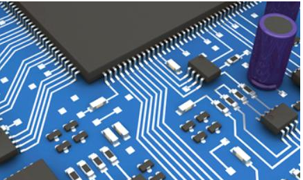
The electrical, mechanical, and thermal behavior of a printed circuit board depends heavily on the materials used in its construction. In addition to copper conductors and electronic components, the selection of PCB Substrate Materials has a direct impact on signal integrity, thermal management, mechanical reliability, and long-term performance.
For conventional applications, standard FR-4 may provide a practical balance between performance and cost. However, high-speed, high-frequency, high-power, and mechanically demanding applications may require more specialized laminate systems.
When selecting a PCB substrate, designers should therefore evaluate the material’s electrical, structural, mechanical, and thermal characteristics rather than selecting a laminate based solely on cost or general marketing specifications.
Different laminate systems can have significantly different properties, even when they are marketed under similar material categories. Material properties may also vary with frequency, resin content, glass style, copper treatment, temperature, and test methodology.
For this reason, designers should work closely with the PCB manufacturer and laminate supplier when selecting materials for demanding applications.
Four Categories of PCB Material Properties
The most important PCB Material Properties can generally be divided into four major categories:
- Electrical properties
- Structural and mechanical properties
- Thermal properties
- Manufacturing and reliability characteristics
These properties are closely interconnected. A material selected for low electrical loss, for example, must also be evaluated for thermal expansion, mechanical reliability, fabrication compatibility, and cost.
Understanding these interactions is especially important for high-speed and high-density PCB designs.
Electrical Properties
Electrical characteristics are critical when a PCB is used for high-speed digital, RF, microwave, or other high-frequency applications.
Among the most important parameters are dielectric constant, dielectric loss, and frequency-dependent electrical behavior.
Dielectric Constant
The Dielectric Constant, commonly represented by Dk or εr, describes how a dielectric material affects electromagnetic wave propagation.
For high-speed PCB design, Dk is important because it influences transmission-line impedance, propagation velocity, signal delay, and the electrical behavior of high-frequency interconnects.
However, the dielectric constant should not be treated as a single fixed value under all conditions. It can vary with:
- Frequency
- Resin content
- Glass weave style
- Material formulation
- Temperature
- Measurement method
- Local laminate structure
The effective Dk experienced by a PCB trace can therefore differ from the nominal material value specified in a datasheet.
Frequency-Dependent Dispersion
In high-speed interconnects, the dielectric properties of a material are frequency-dependent. Different frequency components of a signal may experience different propagation velocities and attenuation.
This behavior is known as dispersion.
For digital signals, which contain a broad range of frequency components, dispersion can contribute to waveform distortion and timing uncertainty. This becomes increasingly important as signal rise times become faster and channel lengths increase.
For high-speed serial links, engineers may therefore need to consider not only nominal Dk but also dielectric loss, frequency-dependent behavior, copper roughness, trace geometry, and the complete channel structure.
Dielectric Loss
Dielectric loss describes the energy dissipated within the dielectric material as an electromagnetic signal propagates through the PCB.
A common parameter used to characterize this behavior is the dissipation factor (Df), or loss tangent.
Lower-loss materials can be beneficial for high-frequency and long-channel applications because they can reduce dielectric attenuation. However, material selection should be based on the complete channel requirement rather than simply choosing the material with the lowest Df.
The PCB stackup, trace geometry, operating frequency, routing length, copper surface treatment, and connector structure can all influence overall channel performance.
Structural and Mechanical Properties
The physical structure of a PCB laminate also affects its electrical and mechanical behavior.
Two important considerations for advanced PCB design are glass weave structure and copper surface roughness.
Glass Weave Effect
PCB laminates are typically reinforced with woven glass fabric embedded in resin.
The glass weave pattern creates regions with different local dielectric characteristics because glass fibers and resin have different electrical properties.
Although the overall laminate may have a specified average Dk, a high-speed trace passing across different portions of the glass weave can experience variations in its local electromagnetic environment.
This phenomenon is commonly referred to as the Glass Weave Effect.
For very high-speed or high-frequency applications, the glass weave effect can contribute to:
- Local impedance variation
- Propagation-delay variation
- Differential-pair skew
- Mode conversion
- Additional signal distortion
The severity depends on frequency, trace geometry, glass style, resin distribution, routing direction, and the specific laminate construction.
Designers can reduce the risk by considering routing orientation, trace-to-glass interaction, differential-pair geometry, and appropriate material construction during stackup development.
For demanding applications such as automotive radar, high-speed networking, data-center hardware, and advanced SerDes channels, glass weave effects may require more careful analysis.
Copper Roughness
Copper Roughness is another important material characteristic for high-speed PCB design.
Copper conductors are not perfectly smooth. The microscopic surface structure of the copper increases the effective path length traveled by high-frequency current.
This becomes particularly important because of the skin effect. As frequency increases, current tends to concentrate near the conductor surface. Greater copper roughness can therefore increase conductor loss and contribute to signal attenuation.
Copper roughness can be influenced by:
- Copper foil type
- Copper treatment process
- Electroplating conditions
- Etching process
- Resin and dielectric interface
- Surface-treatment technology
For high-frequency applications, low-profile or ultra-low-profile copper may be considered when appropriate.
However, the optimal copper surface treatment must also satisfy PCB manufacturing requirements such as adhesion, reliability, plating compatibility, and process stability.
Therefore, copper roughness should be evaluated together with the laminate system and fabrication process rather than as an isolated parameter.
Thermal Properties
Thermal performance becomes increasingly important as PCB power density increases.
When selecting PCB Substrate Materials, designers should consider thermal conductivity, specific heat, glass transition temperature, and coefficient of thermal expansion.
Thermal Conductivity
Thermal Conductivity indicates how effectively a material transfers heat.
A PCB with significant heat generation may require materials and structures that facilitate heat transfer from components into the board and eventually to a heat sink, chassis, or other thermal-management structure.
For conventional FR-4 boards, the dielectric layer generally provides much lower thermal conductivity than copper. As a result, the dielectric material can become a major thermal barrier.
High-thermal-conductivity dielectric materials or metal-core PCB structures may therefore be considered for applications with demanding thermal requirements.
However, simply choosing a material with high thermal conductivity does not automatically solve a thermal problem. The complete thermal path must also be considered:
Component → Copper → Dielectric → Core → Heat Sink / Chassis
Copper area, via arrays, dielectric thickness, interface materials, heat-sink design, and airflow can all affect the final thermal performance.
Specific Heat
Specific heat describes the amount of energy required to raise the temperature of a material by a given amount.
Although specific heat is not normally the primary parameter used for selecting a PCB laminate, it contributes to the board’s thermal response during transient heating and cooling.
For most PCB thermal designs, thermal conductivity, thermal resistance, heat generation, and thermal interfaces are more directly useful for evaluating steady-state temperature performance.
Coefficient of Thermal Expansion
The Coefficient of Thermal Expansion (CTE) describes how much a material expands or contracts when its temperature changes.
PCB laminates are anisotropic materials, meaning their thermal expansion can differ depending on direction.
This is particularly important in multilayer PCBs because the copper, resin, glass reinforcement, and other materials have different CTE values.
When the PCB experiences repeated thermal cycling, differences in thermal expansion can generate mechanical stress.
CTE and PCB Reliability
CTE becomes especially important when designing boards with:
- High layer counts
- Large aspect-ratio plated through-holes
- Microvias
- Blind and buried vias
- HDI structures
- Fine-pitch components
- Lead-free assembly processes
- Multiple thermal cycles
As temperature rises through the material’s glass transition temperature (Tg), the resin system undergoes a significant change in its expansion behavior, particularly in the Z-axis.
A material with a suitable Tg and controlled Z-axis CTE can help improve reliability under thermal cycling.
However, a higher Tg alone does not guarantee better PCB reliability. Designers should evaluate Tg together with Z-axis CTE, decomposition temperature (Td), copper adhesion, moisture resistance, laminate construction, and the expected assembly and operating conditions.
Glass Transition Temperature
Glass transition temperature, or Tg, is another important parameter when selecting laminate materials.
Below Tg, the resin system behaves in a relatively rigid state. Above Tg, its mechanical properties change substantially and thermal expansion increases, particularly in the Z-axis.
For applications exposed to repeated reflow cycles or elevated operating temperatures, a suitable high-Tg material may provide better dimensional stability and thermal reliability than a basic laminate.
Standard FR-4 remains widely used because of its balance of electrical performance, mechanical properties, availability, and cost. However, higher-Tg and specialized laminate systems are available for more demanding applications.
Material selection should always be based on the actual operating and manufacturing temperature profile.
PCB Materials for HDI and High-Density Designs
Advanced PCB Material Properties become particularly important in HDI and high-density applications.
HDI structures often use microvias, sequential lamination, fine lines, and fine-pitch component connections. These structures place greater demands on dimensional stability and interconnection reliability.
For HDI PCB Design, designers may need to consider:
- Laminate CTE
- Tg and thermal stability
- Resin content
- Laser-drilling characteristics
- Desmear compatibility
- Copper plating reliability
- Layer-to-layer registration
- Moisture absorption
- Dielectric thickness
- Dk and Df
- Copper surface profile
The laminate must be compatible with both the electrical requirements of the design and the manufacturing process used to fabricate the HDI structure.
Choosing the Right PCB Substrate
The selection of PCB Substrate Materials should begin with the actual electrical, mechanical, thermal, and environmental requirements of the product.
A practical material-selection process may include the following steps:
1. Define Operating Frequency
Determine the signal frequency, rise time, channel length, and required impedance.
2. Evaluate Electrical Requirements
Review Dk, Df, impedance requirements, dielectric loss, and frequency-dependent behavior.
3. Evaluate Mechanical Requirements
Consider CTE, dimensional stability, board thickness, flexural requirements, and mechanical stress.
4. Evaluate Thermal Requirements
Consider power density, operating temperature, thermal conductivity, thermal resistance, and heat dissipation paths.
5. Consider Manufacturing Capability
The selected material should be compatible with the PCB manufacturer’s lamination, drilling, plating, etching, and assembly processes.
6. Verify Reliability Requirements
Evaluate thermal cycling, moisture resistance, via reliability, CAF resistance where applicable, and expected product lifetime.
7. Consider Cost and Availability
Specialized materials can provide superior electrical or thermal performance but may increase manufacturing cost and procurement complexity.
The best material is therefore not necessarily the most advanced or most expensive one. It is the material that provides the required performance while remaining compatible with manufacturing and commercial requirements.
Working with Kingda on PCB Material Selection
Material selection should ideally be discussed with the PCB manufacturer before finalizing the stackup.
Kingda can support customers in evaluating PCB material requirements according to application conditions, layer count, controlled-impedance requirements, HDI structures, thermal demands, and manufacturing processes.
For high-speed and high-frequency projects, the material selection process can be coordinated with stackup development, impedance calculations, routing requirements, fabrication tolerances, and production capabilities.
This approach helps ensure that the selected laminate is not only suitable from a theoretical electrical perspective but also practical for PCB manufacturing.
Conclusion
The performance of a PCB depends on much more than circuit routing and component selection. PCB Material Properties have a direct influence on electrical behavior, signal integrity, thermal performance, mechanical stability, and long-term reliability.
For high-speed designs, parameters such as Dielectric Constant, dielectric loss, Glass Weave Effect, and Copper Roughness can significantly influence signal behavior. For thermally demanding and mechanically challenging applications, Thermal Conductivity and Coefficient of Thermal Expansion (CTE) become equally important.
FR-4 remains an excellent choice for many conventional PCB applications, but advanced products may require specialized laminate systems with controlled electrical, thermal, and mechanical characteristics.
By evaluating material properties together with stackup design, manufacturing capability, and application requirements, engineers can select a PCB substrate that provides a better balance of performance, reliability, manufacturability, and cost. Kingda can work with customers from material and stackup planning through PCB fabrication to help turn demanding PCB designs into reliable production-ready boards.