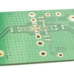
Tin Plating PCB: Surface Finish Process, Benefits and Applications
Tin plating is one of the most established ways to protect the bare copper on a printed circuit board. It has been used for decades in consumer electronics, automotive control modules, power supply boards, and industrial control systems because it offers dependable solderability, good oxidation resistance, and a lower cost than noble metal finishes. For engineers and buyers who manage medium and large production runs, tin plating remains a mainstream choice even as newer finishes appear. This guide explains how tin plating PCB finishes work, the chemistry behind them, their structure and performance limits, quality control methods, and how they compare with alternatives such as ENIG and OSP.
What Is a Tin Plating PCB?
A tin plating PCB is a circuit board whose exposed copper pads and traces receive a thin electroplated tin layer. During the process, tin ions in a plating bath are reduced and deposited onto the copper surface under direct current, forming a dense metallic coating that shields the copper from oxidation. Because tin and copper form metallic bonds and gradually create a copper-tin intermetallic layer, the finish offers better wetting behavior during soldering than organic films such as OSP.
The finish is valued for a practical combination of properties: it is economical, electrically conductive, compatible with both wave and reflow soldering, and lead-free under RoHS requirements. Tin plating is a proven technology, which means suppliers have decades of process data, equipment, and test experience behind it. That maturity is one reason it continues to appear on high-volume boards in appliances, smart home devices, automotive electronics, and industrial equipment.
Core Principles of the PCB Tin Plating Process
Two technical ideas sit at the heart of PCB tin plating. The first is metallurgical bonding. Tin atoms diffuse into the copper base and form an intermetallic compound layer at the interface, which gives the deposit strong adhesion. The second is electrochemical deposition. Tin ions in the plating solution are reduced at the cathode surface under a controlled direct current, where they crystallize into a uniform, compact metal layer.
During electroplating, the main reduction reaction is simple: Sn2+ ions accept two electrons and become metallic tin on the board surface. The quality of that deposit, however, depends on process discipline. Bath pH, ion concentration balance, additive purity, and agitation speed all influence the crystal structure of the layer. When the chemical system drifts out of its window, boards can develop dull surfaces, poor soldering behavior, and oxidation spots that only appear later in assembly or field use.
Structure of a Tin Deposit
A finished tin layer is not a single uniform film but a three-part structure. On top sits a layer of tin crystals whose grain size determines wetting and mechanical behavior. Below that is a copper-tin intermetallic diffusion zone that bonds the deposit to the substrate, and beneath everything is the copper base material. Fine-grained deposits are preferable because they improve solder paste wetting, reduce the probability of whisker growth, and add mechanical toughness to the surface.
Grain structure matters in production because it is controlled by the plating chemistry and current conditions. A brightener system that produces fine, dense grains also tends to produce smoother surfaces that print solder paste consistently. Conversely, coarse or columnar grains indicate a bath that is out of balance and will eventually create soldering and reliability problems on the line.

Electrical and Thermal Performance of Tin Finish
Tin is an excellent electrical conductor, and a properly plated layer maintains low contact resistance on pads and connectors. The finish also reflows well, adapting to the molten solder during assembly so that joints form cleanly across the whole pad. Although the thermal conductivity of tin is lower than that of copper, the plating is only a few micrometers thick, so its effect on board-level heat spreading is negligible. That makes tin plating suitable for LED driver boards, power modules, and other designs where heat management is handled by copper planes and thermal vias rather than by the surface finish.
Signal behavior is another practical concern. At typical plating thicknesses, tin contributes minimal insertion loss and supports stable transmission for control and low-to-medium speed signals. For very high frequency RF designs, engineers usually prefer flatter finishes such as ENIG, but for the majority of digital and analog boards tin plating delivers dependable performance at a fraction of the cost.
Plating Thickness and Its Effect on Reliability
Recommended tin plating thickness for PCB surfaces is generally in the range of 1 to 10 micrometers, with the specific target depending on the application and the customer specification. Too thin a layer leaves the copper poorly protected and increases the risk of weak solder joints, while an excessively thick layer raises internal stress and the risk of whisker formation. Plating thickness is checked with X-ray fluorescence (XRF) instruments and cross-section metallography, and the results should be recorded per panel for traceability.
Uniform thickness across the board is as important as the average value. Current density varies with panel layout, so areas near bus bars and panel edges can plate differently from the center. Good suppliers adjust rack design, current settings, and bath agitation to keep the deposit even, then verify the result with multiple measurement points rather than a single reading.
Tin Whiskers: Causes and Prevention
Tin whiskers are microscopic metallic filaments that can grow from a tin surface over time and create short circuits between adjacent conductors. The phenomenon has been studied intensively because of failures in military, aerospace, and high-reliability electronics. Whiskers grow when internal compressive stress builds up in the deposit, when the crystal lattice is unstable, or when humidity and thermal cycling provide the energy for migration.
Prevention strategies include alloying the tin with small amounts of elements such as bismuth or nickel, applying stress-relief annealing after plating, and controlling grain orientation during deposition. Matte tin finishes with controlled grain structure are generally preferred over bright finishes for high-reliability products. When a project requires the lowest possible whisker risk, designers should discuss the mitigation plan with the PCB manufacturer and define the acceptance criteria in the specification before production begins.
Adhesion, Wetting and Corrosion Resistance
Adhesion between the tin layer and the copper surface depends on surface roughness, cleanliness after pretreatment, and the completeness of the intermetallic layer. If the copper surface carries oxides or organic residue before plating, the deposit will not bond properly and can peel during soldering or thermal cycling. Proper micro-etching and rinsing steps in the pretreatment line are therefore the first line of defense against finish defects.
Good wetting reduces common assembly faults such as cold joints, voiding, and incomplete fillets, which is why tin-plated boards run smoothly on high-speed SMT lines. In service, tin forms a thin, stable oxide film in air that protects the copper from oxidation, sulfur attack, and halogen exposure. This self-limiting oxide layer makes tin plating a reasonable choice for outdoor IoT devices and other environments where boards see moisture and pollutants, although storage life remains shorter than noble metal finishes.

Tin Plating vs. ENIG, OSP and Immersion Silver
Choosing a finish means weighing cost, reliability, solderability, and shelf life together. Tin plating offers excellent cost and good solderability, with moderate storage life. ENIG provides a flat, corrosion-resistant surface with long storage life and excellent reliability, but at noticeably higher cost. OSP is the cheapest option and prints solder well, yet it offers weaker corrosion protection and the shortest shelf life. Immersion silver sits between them: moderate cost, good solderability, and fair reliability, though it can tarnish in sulfur-rich air.
For medium and high volume production of consumer and industrial boards, tin plating is frequently the best balance. It avoids the premium of ENIG while delivering better protection than OSP. Designers who need flatness for fine-pitch BGA assembly or who must store boards for many months should evaluate ENIG; everyone else can usually save money with tin without compromising yield. A capable PCB manufacturing partner will show actual test data for each finish on your specific stack-up, which beats comparing datasheets in isolation.
Key Process Parameters and Common Defects
Plating quality is governed by a handful of parameters: current density, bath temperature, brightener ratio, and circulation speed. If these drift, the line produces localized burning, uneven thickness, rough surfaces, or dull deposits. Common defects seen on poorly controlled lines include plating peeling, surface cracks, localized blackening from oxidation, coarse grain layers, and whisker growth. In most cases the root cause traces back to inadequate pretreatment or unstable bath chemistry rather than to the plating step itself.
Because defects are invisible until soldering or field use, process control is the real product. Bath analysis schedules, ampere-hour tracking, and regular Hull cell testing keep the chemistry inside its window, while first-article inspection after every bath adjustment catches drift before it reaches the customer.
Testing and Standards for Tin-Plated PCBs
Acceptance testing for tin plating follows well-established methods. Metallographic cross-sections reveal layer structure and intermetallic integrity, XRF measures thickness across the panel, and peel or pull tests verify adhesion. Contact resistance measurements confirm electrical performance, and salt spray testing checks corrosion resistance for outdoor products. Suppliers that ship boards to IPC-4552 or equivalent specifications provide documentation for each lot, giving buyers confidence that the finish meets the agreed requirements.
Testing does not stop at the bare board. Assembly-line results are the ultimate proof of solderability, so many buyers run solderability tests and monitor defect rates through their PCBA testing program. Boards that pass electrical test, AOI, and functional test with tin finish typically demonstrate the low field failure rates that justify its use on volume products.
Typical Applications of Tin Plating PCB
Tin-plated boards appear wherever cost-effective, solderable surfaces are needed at scale. Smart home control boards, automotive instrument clusters, communication modules, white-goods main boards, and industrial PLC systems all use tin finish in large volumes. Engineering teams in these industries care most about consistent wetting on the assembly line, because a finish that behaves predictably protects their yield and delivery schedule.
The finish also suits products with moderate storage requirements. When boards are assembled within a few months of fabrication, tin plating provides dependable results without the expense of gold or silver. For companies moving from prototyping to mass production, keeping the same finish family through prototype PCB assembly and into volume manufacturing reduces qualification effort and cost surprises.
Future Trends in Tin Plating Technology
Tin plating is not standing still. The industry is moving toward nano-grain control for better mechanical properties, AI-assisted bath monitoring that predicts chemistry drift before it affects quality, new whisker-resistant alloy systems, and cleaner electroplating chemistries with lower environmental impact. These advances keep tin competitive against noble metal finishes while preserving its cost advantage.
For the foreseeable future, tin plating will remain a strong choice for mid-range and high-volume electronics. Buyers should watch for suppliers that invest in bath analytics and grain-structure control, because those capabilities directly translate into more consistent solder joints and fewer field returns on their products.
Tin Plating PCB FAQ
Q1: How long can a tin-plated PCB be stored? Typical storage life is 6 to 12 months when boards are kept dry, sealed, and away from light. Solderability degrades gradually after that window.
Q2: Is tin plating RoHS compliant? Yes. Conventional electroplated tin processes can be formulated lead-free and meet RoHS requirements, and many suppliers certify their chemistry.
Q3: Can tin plating be used for fine-pitch pads? It can, but ENIG offers better flatness for very dense packages such as fine-pitch BGAs. For most SMT pads, tin plating performs well.
Q4: Does tin plating affect signal integrity? At normal plating thickness the effect is minimal. Tin is conductive and the layer is thin, so it suits standard digital and analog boards; RF designers still prefer flatter finishes.
Q5: Why did my tin boards show dark spots? Darkening usually comes from oxidation after plating or from bath chemistry drift. Check storage conditions, plating thickness, and the pretreatment line with your supplier.
Conclusion
Tin plating PCB finish remains one of the most practical surface treatments for volume electronics. It protects copper, solders dependably, meets environmental requirements, and keeps board cost low. Success depends less on the finish itself than on process control: stable chemistry, uniform thickness, controlled grain structure, and disciplined testing. Working with an experienced manufacturer that documents its plating parameters and test results lets engineers specify tin with confidence, whether the product is a smart home controller, an automotive module, or an industrial system produced by the thousands. Teams that pair the right finish with an SMT PCB assembly line experienced with that finish get the yields and reliability their schedules depend on.