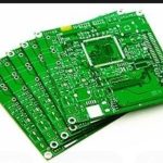
HDI PCB Prototyping: Process, Lead Time and Cost Guide
Rapid Iteration for Dense Boards
Smartphones, wearables, medical electronics, automotive modules, IoT devices and high-speed communications equipment are all shrinking while adding more connections, and that is why hdi pcb prototyping has become a standard step in product development. HDI PCB technology uses microvias, blind and buried vias, fine lines, fine pitch and sequential lamination to pack more electrical connections into a smaller board area. Rapid prototyping with these processes lets engineering teams validate designs, run functional tests and optimize structures in days rather than weeks. This guide explains the HDI quick-turn process, typical lead times, 2026 price ranges, cost drivers, design rules and how to choose a prototyping partner.
Why HDI Prototyping Matters
The value of HDI is density. Microvias occupy far less space than traditional through-holes, freeing routing area under high-pin-count BGAs, CSPs and fine-pitch devices. HDI makes board size smaller, supports high-density packaging with escape routing under large processors, and improves high-speed signal design by shortening interconnects and easing impedance control for USB, PCIe, MIPI, DDR and high-speed Ethernet. Most importantly for development teams, an hdi pcb prototype exposes layout, signal integrity, BGA fanout, power integrity, EMI, assembly and mechanical interference problems early, when fixes are still cheap, and compresses the whole design-validate-iterate cycle.
The HDI Prototyping Process
A complete HDI quick-turn build follows a fixed sequence. Engineering and DFM review comes first: the factory checks Gerber, ODB++, NC drill, stack-up, mechanical dimensions, copper and board thickness, impedance, finish, solder mask and special tolerances, flagging line width, spacing, microvia size, pad size, layer registration and stack-up risks before production. Material selection follows, with standard FR-4, high-Tg, low-loss, high-frequency, halogen-free and special HDI dielectrics chosen by electrical and thermal need. Inner layers are then imaged, etched and AOI inspected before lamination.

Core HDI Processes
Laser drilling is the heart of HDI, forming microvias through thin dielectric layers to connect adjacent conductive layers with smaller holes than mechanical drilling can produce. Sequential lamination then builds 1+N+1, 2+N+2, 3+N+3 or any-layer structures on a conventional core. Copper plating metallizes the microvias through desmear, electroless copper, electrolytic copper and pattern plating, and the quality of hole-wall copper decides interconnect reliability. Outer layer imaging, plating and etching follow with tighter exposure, registration and etch control because HDI uses fine lines and spacing, and the process finishes with surface finish, AOI, electrical test, X-ray, cross-section, dimensional, impedance and solderability checks where required.
Typical Prototyping Lead Times
Lead time scales with complexity. Simple 1+N+1 HDI boards typically prototype in five to seven working days, 2+N+2 designs in eight to fifteen days, and complex or any-layer HDI in ten to twenty working days or longer. Delays usually come from special material procurement, complex stack-ups, many lamination passes, aggressive line width or via sizes, tight impedance tolerances, special finishes, incomplete files, engineering revisions and extra reliability testing. That is why lead time should be judged against manufacturing capability, not against the fastest number a supplier advertises.
2026 Price Ranges for HDI Prototypes
HDI prototyping prices vary with specification, but the following 2026 market ranges are a useful budget reference: simple 1+N+1 HDI runs about USD 80-180 per board, medium-complexity HDI USD 150-300, 2+N+2 HDI USD 200-450, and high-end or any-layer HDI USD 350-800 or more. Prototype prices sit far above volume pricing because engineering setup, tooling and special processes dominate small orders. Treat these figures as planning numbers, and get a real quote from the actual stack-up and files.

What Drives HDI Prototype Cost
Six factors move the price. Layer count raises material, lamination, imaging, drilling, plating and inspection work. HDI structure matters because 1+N+1 is simpler than 2+N+2 or any-layer builds that need repeated sequential lamination. Microvia count increases laser, plating and test effort, but cutting vias blindly to save money is the wrong approach; optimizing stack-up and routing is the right one. Materials matter because standard FR-4 is economical while high-frequency, low-loss and special laminates cost more. Copper weight, surface finish, board size, prototype quantity and expedite requests all add to the bill, with ENIG suited to fine-pitch assembly, OSP cheaper, ENEPIG for high reliability and immersion silver for special high-performance applications.
Design Rules for Fast, Reliable Prototypes
Design choices made before quoting decide how fast and stable the prototype run will be. Microvia size should match dielectric thickness and laser capability, because overly aggressive vias shrink the process window and hurt yield and reliability. Line width and spacing should be relaxed wherever electrical performance allows. Via-in-pad solves BGA fanout but adds via filling, copper fill and planarization steps that raise cost. The stack-up must balance signal, ground and power layers with dielectric thickness, copper and impedance targets, and impedance requirements for USB, PCIe, MIPI, DDR, Ethernet or RF should be agreed before production, not discovered after; a PCB design and layout review catches these issues before tooling.
How to Shorten HDI Lead Time
Prototype speed is mostly controlled by preparation. Choose materials the factory stocks to avoid procurement wait. Freeze the stack-up early, because changing it restarts engineering review. Provide complete production data in one pass, including Gerber or ODB++, NC drill, stack-up, fabrication drawing, impedance requirements, finish, copper, thickness and special notes. Complete DFM review before production so microvia, spacing, stack-up and impedance problems are caught on screen instead of in rework. Finally, select a factory with full in-house HDI capability, including laser drilling, sequential lamination, plating, AOI, X-ray and electrical test, because outsourcing any step makes delivery harder to control.
HDI vs Standard PCB Prototyping
HDI and ordinary multilayer boards are not simply an upgrade of each other. Standard PCB prototyping suits general electronics with moderate routing density, no microvias, limited fine-pitch BGA and relatively larger boards, at lower cost and complexity. HDI quick-turn prototyping suits high-density, miniaturized electronics where space is tight, BGA pin counts are high and routing is dense. If a conventional multilayer board meets the routing and electrical requirements, there is no reason to add HDI complexity; when space is limited and vias are dense, HDI is usually the more sensible route.
Applications and Supplier Choice
HDI prototypes serve consumer electronics such as smartphones, tablets, smartwatches and cameras; automotive electronics such as ADAS and in-vehicle systems; medical devices; IoT hardware; and high-speed communications products. When choosing a quick-turn supplier, verify real HDI process capability, in-house laser and sequential lamination, engineering DFM support, and a documented path from prototype to volume production. A partner offering PCB manufacturing with PCBA testing lets the first prototype become a validated module faster, because board and assembly issues are resolved in one loop.
HDI PCB Prototyping FAQ
Q1: How fast is hdi pcb prototyping? Simple 1+N+1 boards typically take five to seven working days, with complex any-layer builds running ten to twenty days or more.
Q2: How much does HDI prototyping cost? Roughly USD 80-180 for simple 1+N+1 boards up to USD 350-800 plus for any-layer designs.
Q3: What causes HDI delays? Special materials, complex stack-ups, multiple laminations, fine features, tight impedance and incomplete files are the common causes.
Q4: When is HDI necessary? When board space is limited, BGA density is high or routing needs exceed what conventional multilayer boards can deliver.
Conclusion
HDI PCB prototyping turns high-density designs into testable hardware quickly, but speed depends on process capability and preparation. Microvias, sequential lamination and fine features deliver smaller, denser, higher-performance boards, while disciplined DFM and complete files keep lead times and cost under control. Teams that pair good HDI design rules with a factory that owns the full process get prototypes that validate quickly and scale into production without surprises.