




SMT PCB Assembly Terms: BOM, DIP, SMT and SMD Guide
SMT PCB assembly terms such as BOM, DIP, SMT, and SMD are used in almost every electronics manufacturing document. A customer who understands these terms can communicate more clearly with the PCB assembly factory, review the process, and check the product documentation. This guide explains the meaning of each term and how it is used in production.
The electronics industry uses many abbreviations. BOM describes the component list, DIP describes a through-hole package, SMT describes the surface mount assembly technology, and SMD describes the component itself.
Each term represents a different part of the PCB manufacturing and assembly process.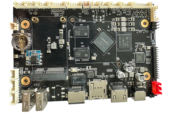
What Is a BOM
BOM stands for bill of materials. It is a document that describes the product structure in a table or matrix form.
The surface mount processing BOM contains the material name, quantity, reference designator, package type, and placement location for every component. It also lists the manufacturer part number when the data is complete.
The BOM is an important basis for placement machine programming. The machine program is built from the component positions and package information in the BOM.
It is also used for integrated quality control. The factory compares the BOM with the incoming materials, the feeder setup, and the assembled board to confirm that every component is correct.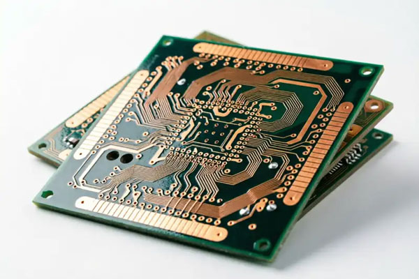
BOM Quality Requirements
A clear BOM should include the component reference, value or specification, package, quantity, and preferred manufacturer part number. Alternate part numbers should be listed when approved.
The BOM should identify polarity-sensitive components and any special process instruction. Missing information can cause the factory to buy the wrong component or place it in the wrong direction.
BOM revisions should be controlled. When the engineering change notice is released, the assembly documentation should be updated at the same time.
If the BOM is not accurate, even a perfect assembly line cannot build a reliable product.
What Is DIP
DIP stands for dual in-line package. It refers to integrated circuit chips packaged with two parallel rows of pins that can be inserted into a socket or through holes on the PCB.
Most small and medium integrated circuits use this packaging form. The pin count usually does not exceed 100, and many DIP components have 8 to 48 pins.
A DIP package can be inserted directly into a chip socket or soldered into plated through-holes on the circuit board. This makes the component easy to replace in prototype and service work.
Because the pins pass through the board, DIP components create a strong mechanical connection and are still used for selected parts.
Advantages and Limits of DIP
DIP components are convenient for manual assembly and testing. A chip inserted into a socket can be removed without desoldering, which is useful during product development.
However, DIP packages occupy a large board area and require drilled holes. They cannot achieve the component density of surface mount packages.
For high-volume products, most integrated circuits are now supplied in surface mount packages rather than DIP. DIP remains important for legacy designs, repair, and low-volume equipment.
What Is SMT
SMT stands for surface mount technology. It is a circuit assembly technology used to connect surface mount components to designated locations on the surface of a printed circuit board.
In the SMT process, solder paste is first coated on the board, then surface mount components are placed accurately on the solder-coated pads. The board is then heated until the solder paste melts and cools, forming the interconnection between the component and the PCB.
During the 1980s, SMT production technology became more complete and component prices fell sharply. High-performance, low-price equipment became widely available.
SMT is now used in aviation, communication, computer, medical, automotive, office automation, and home appliance PCB production.
Advantages of SMT
SMT provides high assembly density, small product volume, and light weight. The volume and weight of a surface mount assembly can be only a fraction of a traditional through-hole assembly.
After surface mounting, the volume of an electronic product can be reduced by 40 to 60 percent, and the weight can be reduced by 60 to 80 percent under the same function.
The surface mount process also supports automation. Pick-and-place machines can assemble thousands of components per hour with high accuracy.
This reduces assembly cost and allows complete, low-priced products to be manufactured on a large scale.
What Is SMD
SMD stands for surface mounted device. It is the component that is mounted by the SMT process.
In the early stage of electronic circuit board production, through-hole assembly was completed manually. After the first automated machines appeared, they could place simple pin components, but complex components still required manual placement and wave soldering.
Surface mount components were introduced later and created a new era. From passive components to active components and integrated circuits, most parts can now be supplied as SMDs and assembled by pick-and-place equipment.
SMD components can be mounted on both sides of the board and do not require a hole for every lead.
Types of SMD Components
SMD components include chip resistors, chip capacitors, chip inductors, diodes, transistors, small outline ICs, BGAs, connectors, and many other package forms.
Passive components are often rectangular chips. Active components use packages such as small outline transistors, small outline ICs, plastic quad flat packs, and ball grid arrays.
The component body can be placed on either side of the PCB, which increases design flexibility and reduces board size.
SMD packages should be selected to match the placement machine capability and the soldering process.
How the Terms Work Together
The BOM tells the factory which SMD components to use and where each component belongs. The placement machine program is generated from this data.
SMT is the assembly technology, while SMD is the component package that the process places. DIP is the older through-hole packaging method still used for selected ICs and connectors.
When the customer and factory discuss a project, they should confirm the BOM, the process type, and the package forms together.
This avoids confusion between a component description and the process used to assemble it.
PCBA Documentation
A professional PCBA project includes the schematic, BOM, assembly drawing, and fabrication drawing. The assembly drawing shows component polarity and placement direction.
The process document defines the SMT or mixed technology process, special soldering requirements, and the test method.
Quality records link the BOM revision to the actual production lot. If a component is changed, the document revision must be updated and confirmed.
Complete documentation reduces the time needed for quoting, purchasing, assembly, and troubleshooting.
A professional PCB assembly service should review the BOM and package list during the DFM process. This review catches missing polarity marks and incorrect footprints before production.
The SMT PCB assembly line then uses the same data to set up feeders, placement programs, and inspection programs.
PCBA testing should verify that the assembled board matches the BOM and the design intent. Testing is especially important when DIP and SMD components are mixed on the same board.
All records should be managed under quality management so the customer can trace every component and process step.
BOM and Component Procurement
The BOM is also used for component purchasing. The factory should check the part number, package, quantity, and lead time for every line in the BOM. When the component is obsolete or has a long lead time, the engineer should identify an approved alternate before the board design is frozen.
Component procurement should be coordinated with PCB component procurement services so that parts arrive in the correct packaging and are suitable for the assembly process. A component with the right electrical value but the wrong package cannot be placed on the board.
Incoming components should be inspected against the BOM before they are stored. This prevents a wrong part from entering the line and creating a defect that is difficult to find after soldering.
Choosing the Right Assembly Method
The decision to use SMT, DIP, or a mix of both should be made during design. The assembly method affects the cost, size, and reliability of the product. Most modern boards use SMT for the majority of components and DIP or through-hole for connectors and power parts.
The PCB should be designed so that the selected components can be placed and soldered with the available process. The PCB design and layout team should review pad geometry, component spacing, and process compatibility during the DFM review.
A clear understanding of the assembly terms helps the customer and factory select the most efficient method for every project. It also reduces quoting errors and prevents misunderstanding about which components will be supplied by the customer and which will be purchased by the assembly service.
Conclusion
BOM, DIP, SMT, and SMD are core terms in PCB assembly. The BOM defines the component list, DIP describes through-hole packaging, SMT describes the assembly method, and SMD describes the component package.
Understanding these terms helps engineers and customers review project documents and communicate with the factory. A clear document package is the first step toward a reliable PCBA.
When the BOM, packages, and process are correct, the assembled board meets the design specification and can be manufactured efficiently.


