




PCBA Processing Principles and DFM Checklist
PCBA processing principles help engineers create boards that are easy to assemble, reliable in use, and low in manufacturing cost. A board designed without considering the assembly process may require extra processes, expensive fixtures, or unnecessary rework. Design for manufacturability turns the process requirements into simple PCB layout rules.
Many PCBA problems begin in the design stage. Package selection, pad geometry, component spacing, solder mask, and process route all affect the final yield. The design team should review each of these areas before releasing the PCB files.
This guide explains eight principles of PCBA process design and lists the important points to check in a DFM review.
Principle 1: Prefer Surface Mount and Crimp Components
Surface mount parts and crimp components generally have good processability. With modern package technology, most components can be purchased in a package suitable for reflow soldering.
Some plug-in components can be supplied in versions designed for reflow soldering, including through-hole packages that can be reflowed. If the whole design can use surface assembly, production efficiency and quality improve significantly.
Crimp components, mainly multipin connectors, also have good manufacturability and reliable connections. The design should select these package categories when the product requirements allow it.
Principle 2: Control Package Mix and Pin Spacing
Package size and pin spacing are the most important factors affecting the entire PCB process. A board that mixes many different package types may need a stencil design that cannot satisfy all of them.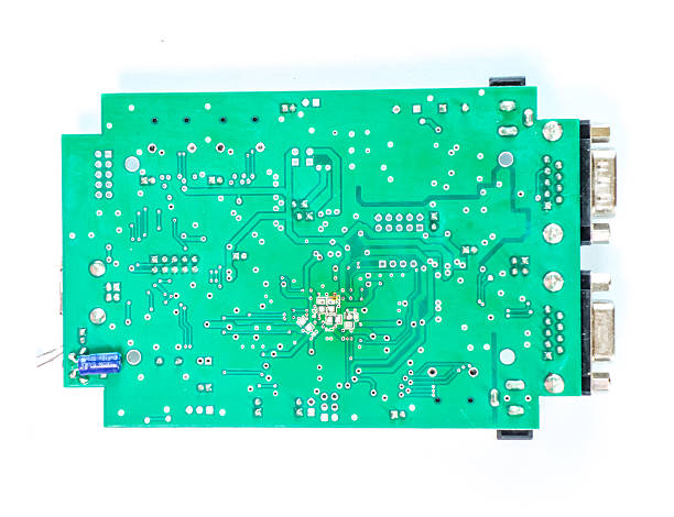
Before layout, the engineer should choose a group of packages with similar or appropriate technical performance. The selected packages should be compatible with one stencil thickness and one board density.
For example, a mobile phone board may use packages that can be printed with a 0.1 millimeter stencil. If the design introduces a very different package type, the engineer should review the stencil plan before continuing.
Principle 3: Shorten the Process Route
A shorter process route gives higher production efficiency and more reliable quality. Each additional process step adds handling, risk, and cost.
In order of preference, the design should use single-sided reflow, double-sided reflow, double-sided reflow plus wave soldering, double-sided reflow plus selective wave soldering, or double-sided reflow plus manual soldering.
The best process is the simplest one that can satisfy the electrical, mechanical, and reliability requirements. Manual soldering should be used only for parts that cannot be processed automatically.
Principle 4: Optimize Component Layout
Component layout covers the arrangement direction and spacing of parts on the board. The layout must satisfy the soldering process and allow the placement machine to work efficiently.
Components that must be soldered by hand should be placed near the board edge and with enough clearance for the operator. Reflow components should be placed so that they do not shadow other parts from heat.
Scientific and reasonable layout can reduce the use of wrong soldering tools and joints. It also makes it possible to optimize the steel mesh and stencil design.
Principle 5: Coordinate Pads, Solder Mask, and Stencil
The pad design, solder mask opening, and stencil window together determine how solder paste is distributed and how the joint forms. They should be designed as one system rather than as separate features.
If the pad is smaller than the mask opening, solder can flow onto the mask and create bridges. If the stencil aperture is too large, the board may receive more paste than the joint needs.
The design should be reviewed so that every pad has a matching mask opening and stencil aperture. A controlled solder paste volume improves wetting and reduces solder balls and bridging.
Principle 6: Qualify New Packages Carefully
New packages are not necessarily new products on the market. A package is new when the factory has no experience using it. For example, a package used by another company may still require qualification for your board and process.
New packages should be introduced in small verification lots before they are used in high-volume production. The engineer should understand the process characteristics, likely problem areas, and countermeasures.
Using a package without qualification can create a defect that appears only after a large quantity has been produced.
Principle 7: Focus on Stress-Sensitive Components
BGAs, chip capacitors, and crystal oscillators are typical stress-sensitive components. Board bending and deformation should be avoided during soldering, assembly, workshop transfer, transportation, and use.
Ceramic capacitors can crack when the board is flexed. BGA balls can fail when the board is bent after assembly. The crystal oscillator package can be damaged by excessive mechanical stress.
The design should keep stress-sensitive parts away from board edges, mounting holes, and high-flex areas. The assembly process should support the board so that no component is bent during handling.
Principle 8: Improve Rules From Case Studies
Manufacturing design rules come from production practice. When a poor assembly or field fault occurs, the design team should update the DFM rules so the same problem is not repeated.
A case study should include the defect image, root cause, process data, and design change. The updated rule should be shared with all designers and reviewed during new product introduction.
Continuous improvement of the design standard reduces the cost of poor quality and increases the success of the next project.
DFM Checklist: Board Construction
The number of PCB layers should be minimized. A single-sided board can sometimes replace a double-sided board, and a double-sided board can replace a multilayer board when the routing density allows it.
Using fewer layers reduces PCB processing cost, but the electrical and mechanical requirements must still be satisfied. The layer reduction should be reviewed with the circuit design engineer.
The board should also meet the requirements of the SMT equipment and process. The dimensions, thickness, and warp tolerance must fit the printer, placement machine, and reflow oven.
The shape and size of the PCB should be correct. Small boards should consider panelization or splicing so that the SMT line can process several circuits together.
DFM Checklist: Tooling and Reference Features
Check that the edge clamping design and locating holes are correct. Tooling holes should be compatible with the printer, placement machine, and test fixture.
Locating holes and non-grounding mounting holes should be marked as nonmetallic when required. A metal mounting hole can short a trace or create an unwanted ground connection.
The fiducial pattern and its position should meet the assembly requirement. A clearance of about 1 to 1.5 millimeters should be reserved around the fiducial and outside the solder mask area.
DFM Checklist: Material and Components
Check whether the base material, component types, and packaging meet the product requirements. The board material must support the operating temperature, signal frequency, and mechanical environment.
Component selection should consider the soldering process, storage requirements, and environmental requirements. Lead-free products need materials and finishes that are compatible with the lead-free profile.
The PCB should use a no-clean process whenever possible to reduce the number of manufacturing steps. Environmental requirements may also affect the selection of solder mask, flux, and cleaning chemicals.
DFM Checklist: Pads, Traces, and Layout
Check that the pad structure, including shape, size, and spacing, follows the DFM specification. The pad geometry must provide enough soldering area without creating bridges between adjacent leads.
The trace width, shape, and spacing should be correct. Trace-to-pad connections should be checked so that solder does not flow away from the joint or into an oversized copper area.
The general component layout and minimum spacing should follow the assembly specification. Large components should leave enough room for rework, and polar parts should be arranged in the same direction when possible.
DFM Checklist: Holes and Manual Operations
For through-hole parts, check that the hole diameter and pad design meet the DFM specification. The plated hole must be large enough for the lead and small enough for the solder to fill the barrel.
Components that are soldered manually should be spaced so that the operator can reach the joint with an iron. Adjacent through-hole parts should not block each other.
The solder mask and silkscreen pattern should be correct, and component polarity and IC pin one should be marked clearly. Clear markings reduce assembly errors and make inspection easier.
Using DFM Feedback in Production
DFM should not stop when the files are released. The SMT factory should review the board during first article production and report any layout problems to the design team.
The SMT PCB assembly process is easier to control when the design uses reflow soldering instead of wave soldering wherever possible. Reflow gives more uniform heating and better support for fine-pitch packages.
Pad, solder mask, and stencil designs should be reviewed together by the PCB design and layout team and the assembly engineer before the stencil is ordered.
First article inspection and PCBA testing confirm that the process route and component layout are correct. Any failures should be documented and added to the DFM lessons learned.
A reliable PCB assembly partner should participate in the DFM review so that manufacturing experience is used during design.
The DFM process should be part of the factory quality management system, with updated rules shared across all new projects.
Conclusion
PCBA processing principles help designers choose packages, layout, process routes, and DFM features that lead to high yield. The eight principles described here cover the most important manufacturability decisions.
The DFM checklist adds specific checks for board construction, tooling, materials, pads, traces, component layout, and manual soldering. Reviewing these points before release prevents many process defects.
When designers and manufacturers share experience and update the design rules, PCBA processing becomes faster, less costly, and more reliable.


