SMT PCB Design Process: Schematic to Layout Guide
The SMT PCB design process takes an electronic circuit from a schematic diagram to a finished board that can be manufactured and assembled. The process includes circuit design, PCB file creation, board planning, component layout, routing rules, and output generation. A clear process reduces design errors and improves the manufacturability of the board.
Most PCB projects begin with a functional requirement. The engineer creates the schematic to show how components are connected, then transfers that information to the PCB layout environment.
This guide explains the main steps in the SMT PCB design process and what the designer should do at each step.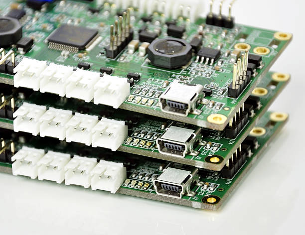
Step 1: Design the Schematic
The first step is to design the electrical schematic. The engineer uses PCB design software to draw the circuit schematic and compile it to generate a netlist.
The netlist describes which component pins must be connected together. It is the logical link between the schematic and the physical board layout.
The schematic should include the component reference designators, values, and pin connections. It should also show power, ground, and signal naming clearly.
Before the layout begins, the schematic should be reviewed for missing connections, incorrect pin assignments, and power problems.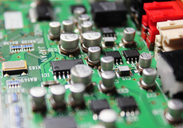
Step 2: Create the PCB File
After the schematic is complete, the designer creates a PCB file. The PCB editor is opened and the board design is carried out in the PCB editing environment.
The PCB file contains the physical board size, layer stackup, component footprints, and copper routing data.
Most PCB software links the schematic and PCB file, so changes made in one document can be synchronized with the other.
The correct software template and unit system should be selected before the board design begins.
Step 3: Plan the Circuit Board
Before drawing the printed circuit board, the designer should plan the board. Planning includes defining the size and shape of the circuit board, setting the layer structure, and setting the design parameters.
The board outline should consider the enclosure, mounting holes, connectors, and assembly process. The layer count should be selected according to the routing density and signal requirements.
The stackup should define copper weight, dielectric thickness, and controlled impedance layers for high-speed signals.
Board planning is an extremely important task because it creates the basic framework for all later layout work.
Step 4: Load the Package Library and Netlist
To place a component on the PCB, the designer must first load the package library for that component. If the library is not loaded, the schematic information cannot be imported into the PCB correctly.
Each footprint in the library should match the physical component. Pad size, spacing, and polarity marks must be correct for the selected part.
After the libraries are loaded, the netlist is imported into the PCB editor. The software places the components and nets in the design database.
If a component footprint is missing, the designer should create it and verify the dimensions before continuing.
Step 5: Place Components
Layout is the process of placing components in the proper positions on the printed board. The word proper has two meanings.
First, the component positions should let the whole circuit board satisfy the electrical signal flow and anti-interference requirements. The board should also look clean and organized.
Second, the component locations should be favorable for routing. Components that must connect to each other should be placed near each other whenever possible.
High-speed, analog, and power circuits should be separated to avoid interference. Decoupling capacitors should be placed close to their IC pins.
Component Placement for Assembly
The placement plan should also consider the SMT assembly process. Components should be oriented so that the placement machine can reach them easily.
Polarity-sensitive parts should be placed in the same direction when possible. Reflow components should not shadow each other from the solder paste printer or the reflow oven.
The board should have fiducial marks for the placement and inspection systems. Large components should leave enough room for rework.
Component placement and DFM rules should be reviewed before routing begins.
Step 6: Set Routing Rules
For components and networks with special requirements, the designer should set routing rules before routing. Rules include safety spacing, trace width, routing layer, and via style.
Power and ground nets may need wider traces to carry current. High-speed nets may need controlled impedance and matched length.
Clearance rules prevent a trace from coming too close to a pad, via, or another trace. The rules should match the manufacturing capability of the PCB factory.
Setting the rules early prevents many routing errors that are difficult to correct later.
Step 7: Route the Board
Routing is the process of laying copper traces to realize the electrical connection between pads. The traces can be routed automatically or manually.
Modern PCB design software has powerful automatic routing. If the component layout is reasonable and the routing rules are correct, the automatic router can complete most of the board.
Manual routing is used to adjust critical signals, clock traces, power paths, and areas where automatic routing creates a conflict.
The routed board should be reviewed for opens, shorts, missing connections, and clearance violations.
Step 8: Generate Reports and Output Files
After the circuit board routing is complete, the PCB file should be saved and checked. The designer should generate the reports needed by the PCB factory and the assembly factory.
Common output files include Gerber data, drill files, the BOM, the centroid file, and the assembly drawing. The Gerber data defines the copper, solder mask, silkscreen, and outline layers.
The centroid file gives the component position and rotation data used by the SMT placement machine.
All output files should use the same board revision and should be checked before they are sent to production.
DFM Check Before Release
Before the design is released, a DFM check should confirm that the board can be manufactured and assembled. The check should cover pad size, solder mask, silkscreen, trace spacing, and hole design.
The PCB design and layout team should work with the manufacturing and assembly engineers to resolve any conflict found in the review.
After the files are released, the PCB manufacturing factory fabricates the bare board and the SMT PCB assembly service assembles the components.
The final board should be verified by PCBA testing to confirm that the design process produced the intended function.
Design changes should be controlled through the quality management process so that every revision is documented.
Design for Testability
The PCB design process should include testability from the beginning. Test points should be added for ICT when the board will be electrically tested with a bed-of-nails fixture. Each test point should have enough spacing and should be connected to a net that needs verification.
If the board is too dense for ICT test points, the design should plan for AOI, X-ray, or flying probe testing. The inspection method should be selected before the layout is finished so that components do not hide critical joints.
Power and ground nets should include a way to measure voltage at the final assembly. A small test pad can save hours of troubleshooting during product development.
High-Speed and Signal Integrity Planning
High-speed signals require controlled impedance traces, return paths, and layer planning. The designer should identify clock, data, and RF traces during the layout and keep them away from noisy switching circuits.
Vias create parasitic capacitance and inductance. High-speed traces should use a small number of vias and continuous reference planes. Ground vias should be placed beside signal vias when the trace changes layer.
The length of a high-speed trace should be matched within the timing requirement of the interface. Differential pairs should be routed together with a consistent spacing.
Signal integrity simulation should be used when the product operates at high frequency or high data rate. Simulation can reveal reflection, crosstalk, and impedance problems before a board is produced.
Version Control and Handoff
The PCB design should be stored in a controlled version system. Each revision should have a unique number and a list of changes. The schematic, layout, BOM, and output files must match the same revision before production begins.
When the design is handed to the factory, the engineer should provide the fabrication drawing, assembly drawing, stackup, and special process notes. Clear handoff documentation reduces questions and delays.
The factory should send a DFM report back to the designer. The report should identify clearance problems, unsupported pads, and other issues that the computer check may not show. Each item should be answered with an action or a technical reason before the files are accepted.
The designer should review the report and correct any issue that can affect assembly yield or reliability.
Engineering change notices should be reviewed by design, manufacturing, and quality before the next board revision is released.
Conclusion
The SMT PCB design process connects the schematic, component libraries, board planning, layout, routing, and output files into one controlled workflow. Each step builds on the previous one.
Reasonable layout and clear routing rules make the board easier to fabricate, assemble, and test. A design review before release prevents many manufacturing problems.
Following the design process carefully gives the product a reliable start from the first PCB sample to high-volume production.