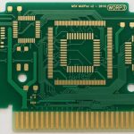
The basic operating principle of a printed circuit board is straightforward. An insulating substrate separates conductive copper layers and provides a controlled structure for electrical connections. Copper traces create predefined current paths between electronic components, allowing the circuit to perform functions such as signal processing, amplification, attenuation, modulation, demodulation, switching, and control.
For beginners, however, one common source of confusion is the difference between a PCB Schematic and PCB Design. Although these two stages are closely related, they serve very different purposes.
A schematic describes what is electrically connected to what, while PCB design determines where those components and connections physically exist on the board.
Understanding this distinction is essential for creating reliable and manufacturable circuit boards. This article explains the differences between a PCB Schematic, PCB Design, and PCB Design Files, as well as how these stages work together in the overall PCB Design Process.
What Is a PCB?
A printed circuit board (PCB) is a structural and electrical platform used to mechanically support and electrically interconnect electronic components.
A typical PCB consists of several major elements, including:
- Insulating substrate materials
- Copper conductive layers
- Copper traces
- Pads and vias
- Solder mask
- Silkscreen
- Through-holes and other interconnection structures
Depending on the application, a PCB may be single-sided, double-sided, or multilayer. Advanced products may also use HDI structures, rigid-flex construction, or flexible PCB technology.
The primary function of a PCB is to provide controlled electrical connections while also meeting mechanical, thermal, manufacturing, and reliability requirements.
What Is a PCB Schematic?
A PCB Schematic is a logical representation of an electronic circuit. It uses standardized symbols and electrical connection lines to describe how components are interconnected.
For example, a schematic may show:
- Microcontrollers
- Resistors and capacitors
- Diodes and transistors
- Connectors
- Power supplies
- Sensors
- Integrated circuits
- Communication interfaces
The schematic focuses on electrical relationships rather than physical positions.
A resistor may be placed on one side of the schematic while its actual PCB footprint is located somewhere completely different on the finished board. This is normal because the schematic is intended to make the circuit logic easy to understand.
The schematic therefore acts as an electrical blueprint for the subsequent PCB Design Process.
What Is PCB Design?
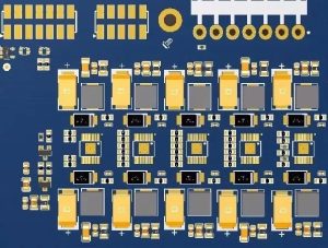
PCB Design converts the electrical information in the schematic into a physical board structure.
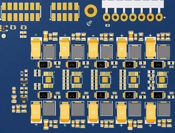
At this stage, engineers determine the physical location of components, copper routing, vias, board layers, power distribution, grounding structures, and other mechanical details.
A typical PCB Design includes:
- Component placement
- Copper trace routing
- Via placement
- Pad and footprint definitions
- Layer stackup
- Power and ground planes
- Board outline
- Mounting holes
- Connector locations
- Silkscreen information
- Design-rule constraints
Therefore, while a schematic answers “How should the circuit be connected?”, PCB design answers “How should those connections be physically implemented?”
This distinction becomes especially important in high-density and high-speed circuit boards.
PCB Schematic vs. PCB Design
The difference can be summarized as follows:
| PCB Schematic | PCB Design |
|---|---|
| Describes electrical relationships | Describes physical implementation |
| Uses schematic symbols | Uses physical component footprints |
| Focuses on circuit logic | Focuses on layout and routing |
| Components are not physically positioned | Components have defined X/Y locations |
| Wires represent logical connections | Copper traces represent physical connections |
| Generally not drawn to physical scale | Must follow actual dimensions |
| Used to verify circuit connectivity | Used to verify manufacturability and physical performance |
In other words, the schematic represents the logical structure, while the PCB design represents the physical structure.
Both are essential, but they solve different engineering problems.
Key Elements of a PCB Schematic
A well-developed PCB Schematic should clearly communicate the electrical architecture of the circuit.
1. Component Symbols
Each component is represented using an appropriate schematic symbol. The symbol identifies the component and its electrical terminals.
For complex systems, components are often grouped by function, such as:
- Power management
- Analog circuits
- Digital processing
- Communication interfaces
- RF circuits
- Sensor circuits
- Control circuits
This organization makes large schematics easier to understand and maintain.
2. Electrical Connections
Connection lines, labels, buses, and net names define how components communicate with each other.
Unlike physical copper traces, schematic connections do not need to follow the actual routing path that will eventually be used on the PCB.
For example, two schematic lines may cross without creating an electrical connection if the schematic conventions indicate that they are separate nets.
3. Component References and Values
Components normally include reference designators and relevant values.
Examples include:
- R1, R2 for resistors
- C1, C2 for capacitors
- U1, U2 for integrated circuits
- L1 for inductors
- D1 for diodes
- J1 for connectors
These identifiers are later associated with physical PCB Components and assembly documentation.
4. Hierarchical and Functional Organization
Large circuit designs may be divided into functional blocks or multiple schematic pages.
This approach allows engineers to separate complex systems into manageable sections while maintaining logical relationships between them.
Important Characteristics of a PCB Schematic
Because a schematic is primarily a logical representation, it does not necessarily resemble the physical PCB.
Several characteristics are important to understand:
- The schematic is generally not drawn to physical scale.
- Components can be arranged for readability rather than physical proximity.
- Electrical connection lines may cross.
- A connection can be represented using net labels instead of long wires.
- Large designs may span multiple schematic pages.
- Functional blocks can be separated into different sections.
Consequently, the visual appearance of a schematic may be completely different from the finished circuit board.
Key Elements of PCB Design Files
After the schematic has been verified, the information is transferred into the physical PCB Design Files.
These files contain the information required to create the actual PCB layout and eventually manufacture the board.
Depending on the design software and manufacturing requirements, PCB Design Files may include:
- PCB layout data
- Component footprints
- Copper layers
- Solder mask layers
- Silkscreen layers
- Drill data
- Board outline
- Stackup information
- Net information
- Design-rule constraints
- Manufacturing outputs such as Gerber or ODB++ data
The exact file formats depend on the CAD system and the requirements of the PCB manufacturer.
Component Placement in PCB Design
One of the most important stages of PCB Layout is component placement.
Unlike a schematic, every component on the PCB must have a specific physical location.
Engineers need to consider:
- Electrical performance
- Signal flow
- Power distribution
- Thermal management
- Mechanical constraints
- Assembly accessibility
- Connector positioning
- Component height
- Manufacturing requirements
For example, high-speed interface components should generally be positioned to minimize unnecessary interconnect length, while switching power components require careful placement to control high di/dt current loops.
Sensitive analog circuits may also need appropriate separation from noisy digital or switching circuits.
PCB Routing and Physical Connections
After placement, engineers create copper routes between pads and vias.
This is where the logical connections defined by the PCB Schematic become physical electrical structures.
Unlike schematic lines, PCB traces must obey actual physical constraints.
Engineers need to consider:
- Trace width
- Trace spacing
- Copper thickness
- Layer transitions
- Via dimensions
- Controlled impedance
- Differential-pair geometry
- Return-current paths
- Crosstalk
- Thermal requirements
- Manufacturing tolerances
For high-speed designs, routing is not simply a matter of connecting two points. Trace geometry, reference planes, impedance, discontinuities, and return-current paths can directly affect Signal Integrity.
PCB Layer Management
Modern PCBs may contain multiple copper layers to accommodate complex routing and power distribution.
A multilayer board may include:
- Signal layers
- Power planes
- Ground planes
- Mixed-purpose routing layers
Using multiple layers allows engineers to route dense designs while maintaining appropriate electrical separation.
However, simply increasing the number of layers does not automatically improve performance. The layer stackup must be designed according to signal speed, impedance requirements, power distribution, thermal considerations, and manufacturing capability.
Thermal and Mechanical Considerations
A major difference between a schematic and physical PCB Design is the need to consider the real-world environment.
The schematic does not show whether two components are physically too close to each other. PCB layout must address these issues.
Engineers may need to consider:
- Component-to-component clearance
- Heat-generating component locations
- Copper area for heat spreading
- Thermal vias
- Heat sinks
- Board-edge clearance
- Connector accessibility
- Mounting-hole locations
- Enclosure restrictions
- Mechanical interference
For power electronics and high-density products, thermal design can be particularly important because excessive temperature can reduce component life and PCB reliability.
The Role of the PCB Silkscreen
The silkscreen is another physical layer that generally does not have a direct equivalent in the schematic.
It can contain:
- Component reference designators
- Polarity indicators
- Pin-1 markers
- Connector labels
- Assembly instructions
- Warning symbols
- Product identification
A properly designed silkscreen helps manufacturing personnel and technicians identify components and orientation during assembly, inspection, testing, and maintenance.
From PCB Schematic to PCB Manufacturing
The complete workflow generally follows this sequence:
Circuit Requirements → PCB Schematic → Component Selection → PCB Layout → Design Rule Check → Simulation/Verification → Manufacturing Data → PCB Manufacturing → PCB Assembly → Testing
The PCB Schematic establishes the electrical intent.
The PCB Layout transforms that intent into a physical arrangement.
The completed PCB Design Files then provide the manufacturing information required to fabricate the board.
Before releasing the design for PCB Manufacturing, engineers should perform appropriate checks, including:
- Electrical rule checking
- Design rule checking
- Footprint verification
- Netlist comparison
- Clearance verification
- Manufacturing capability checks
- Signal integrity analysis where required
- Power integrity analysis where required
- Thermal analysis where necessary
This verification process helps identify problems before the design reaches production.
Why PCB Design Is Critical to Performance
A circuit can be electrically correct at the schematic level but still perform poorly after physical implementation.
For example, a high-speed circuit may have the correct logical connections but experience:
- Impedance discontinuities
- Excessive crosstalk
- Poor return-current paths
- Excessive via stubs
- Power distribution problems
- Electromagnetic interference
- Timing issues
Similarly, a power circuit may have the correct schematic but suffer from excessive voltage drop or temperature rise because of inadequate copper width, poor component placement, or insufficient thermal paths.
Therefore, PCB Design is not simply the process of drawing traces. It is the process of translating electrical requirements into a manufacturable physical structure that satisfies electrical, mechanical, thermal, and reliability requirements.
PCB Schematic and PCB Design Work Together
It is important not to view the schematic and layout as completely independent processes.
They form an interconnected engineering workflow.
A change in the schematic may require changes to the PCB layout. Conversely, physical constraints discovered during layout may require engineers to revisit the schematic or component selection.
For example, engineers may discover that:
- A selected component does not have a suitable package.
- A connector cannot fit within the enclosure.
- A high-speed trace cannot meet the required impedance.
- A power path requires additional copper.
- A thermal requirement cannot be achieved with the current placement.
- A component requires additional clearance.
These issues may require iterative changes before the design can be released for production.
How Kingda Supports PCB Manufacturing
A reliable PCB manufacturing partner should be involved early enough to identify manufacturing risks before production.
At Kingda, PCB manufacturing considerations can be incorporated into the design review process, including material selection, layer structure, line and space capability, via technology, board thickness, copper thickness, surface finish, tolerances, and other production requirements.
For complex boards, early communication between the PCB designer and manufacturer can help reduce unnecessary redesigns and improve manufacturability.
This is especially important for high-density, multilayer, HDI, high-speed, and other advanced PCB applications.
Conclusion
A PCB Schematic and PCB Design are two essential but different stages of electronic product development.
The schematic defines the electrical logic and connectivity, while the physical design determines the component placement, routing, layer structure, and manufacturing implementation.
A successful PCB Design Process therefore requires more than simply creating a correct schematic. Engineers must also consider signal integrity, power integrity, thermal performance, mechanical constraints, manufacturing capabilities, assembly requirements, and long-term reliability.
By clearly understanding the relationship between the PCB Schematic, PCB Layout, and PCB Design Files, designers can create circuit boards that are not only electrically functional but also manufacturable, reliable, and suitable for real-world applications.
With appropriate design verification and early collaboration with a capable PCB manufacturer such as Kingda, the transition from circuit concept to production-ready PCB can be more efficient and predictable.