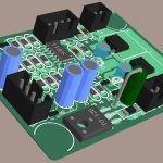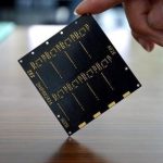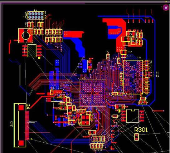
The electronics industry continues to evolve toward smaller form factors, higher integration, faster data transmission, greater power density, and improved reliability. These trends are driving significant advances in printed circuit board technology and creating new challenges for engineers.
Modern PCB Design is no longer limited to simply connecting electronic components. Designers must consider electrical performance, thermal management, mechanical constraints, signal integrity, manufacturability, assembly requirements, and long-term reliability at the same time.
As PCB technology becomes increasingly sophisticated, even relatively small design mistakes can result in difficult assembly, signal problems, manufacturing delays, or expensive redesigns.
Understanding both the major PCB Design Trends and the most common design mistakes can help engineers create more reliable and manufacturable circuit boards.
Major PCB Design Trends
1. Advanced IC Packaging and Higher Interconnect Density
The continuous development of semiconductor packaging is one of the major forces influencing PCB technology.
Advanced packages such as CSP, WLCSP, BGA, QFN, and other fine-pitch packages require increasingly precise PCB footprints and solder-pad structures.
Compared with larger traditional packages, advanced packages can provide:
- Smaller package footprints
- Shorter electrical interconnections
- Higher I/O density
- Improved electrical performance
- Better suitability for compact electronic products
However, these advantages also place greater demands on PCB Design.
Fine-pitch packages require accurate land patterns, controlled solder-mask design, appropriate pad dimensions, and sufficient manufacturing capability.
For high-density packages, engineers may also need to consider microvias, via-in-pad structures, sequential build-up processes, and advanced substrate materials.
Therefore, the development of semiconductor packaging and PCB technology is closely interconnected.
2. Optical and High-Speed Interconnect Technologies
As data rates continue to increase, traditional copper interconnects face challenges related to insertion loss, attenuation, crosstalk, electromagnetic interference, and transmission distance.
This has encouraged the development of optical and electro-optical interconnect technologies.
Optical interconnects can provide important advantages for certain high-bandwidth applications, including:
- High data bandwidth
- Low signal attenuation over appropriate distances
- Reduced susceptibility to electromagnetic interference
- High-density interconnection
- Support for high-speed data communication
These technologies are particularly relevant to data centers, networking equipment, high-performance computing, telecommunications, and other bandwidth-intensive systems.
At the same time, copper remains essential for many PCB applications. Consequently, modern PCB development increasingly focuses on selecting the appropriate interconnect technology according to data rate, distance, cost, power consumption, and system architecture.
3. Rapid Development of Rigid-Flex PCB Technology
Rigid-Flex PCB technology combines rigid PCB sections with flexible circuit sections within a single interconnected structure.
This allows designers to replace multiple boards, connectors, and cable assemblies with a more integrated solution.
The major advantages of rigid-flex construction include:
- Reduced connector count
- Improved packaging efficiency
- Three-dimensional assembly capability
- Reduced wiring complexity
- Potential weight reduction
- Improved mechanical integration
- Increased reliability in suitable applications
Rigid-flex technology is widely used in applications such as:
- Smartphones
- Digital cameras
- Wearable electronics
- Medical devices
- Automotive electronics
- Aerospace equipment
- Industrial instruments
However, rigid-flex boards require specialized design considerations.
Engineers must consider bend radius, bend area, stiffener design, copper type, layer construction, flex-zone geometry, material selection, and dynamic or static bending requirements.
As electronic products continue to become smaller and more mechanically integrated, Rigid-Flex PCB technology is expected to remain an important part of advanced PCB development.
4. High-Layer-Count and High-Density PCBs
High-density electronic systems increasingly require more routing resources within limited board dimensions.
A multilayer PCB provides additional routing layers and dedicated power and ground structures, making it possible to support complex electronic systems.
High-layer-count boards are commonly used in:
- Network switches
- Routers
- Servers
- High-performance computing systems
- Telecommunications equipment
- Industrial control systems
- Advanced automotive electronics
Modern high-density PCB development also involves technologies such as:
- Fine-line routing
- Microvias
- Blind vias
- Buried vias
- Sequential lamination
- Via-in-pad
- Controlled impedance
- Advanced stackup structures
The increasing layer count also makes registration accuracy, lamination control, dielectric thickness, and manufacturing tolerances increasingly important.
A high-layer-count design should therefore be developed together with the manufacturer’s actual process capability.
5. High-Speed and High-Frequency PCB Development
Modern communication, computing, automotive, and RF systems require increasingly higher signal frequencies and data rates.
As signal speed increases, PCB interconnects become part of the electrical system rather than simply passive connections.
Engineers need to consider:
- Controlled impedance
- Differential-pair routing
- Return-current paths
- Crosstalk
- Via discontinuities
- Via stubs
- Dielectric loss
- Copper roughness
- Reference planes
- Connector transitions
- Signal attenuation
This makes signal integrity an increasingly important part of PCB Layout.
Simulation and measurement may also be required to verify that the PCB channel meets the system’s electrical requirements.
6. HDI PCB Technology
HDI PCB technology is another major development direction for compact and high-density electronic products.
HDI uses technologies such as microvias, fine-line routing, sequential build-up, and high-density interconnections to increase routing density within a limited board area.
HDI technology can provide:
- Higher wiring density
- Smaller via structures
- Shorter interconnect paths
- Improved packaging flexibility
- Better utilization of PCB space
- Support for fine-pitch components
HDI is widely used in mobile devices, compact consumer electronics, networking equipment, automotive electronics, medical equipment, and other high-density applications.
However, HDI also introduces additional manufacturing requirements. Laser drilling, microvia plating, sequential lamination, registration accuracy, dielectric selection, and reliability testing all need to be carefully controlled.
Common PCB Design Mistakes
Although PCB technology continues to advance, many production problems still originate from basic design errors.
The following are several common mistakes that engineers should avoid.
1. Incorrect PCB Footprints
A PCB footprint defines the physical land pattern used to mount a component.
Although most EDA software includes extensive component libraries, engineers should not assume that every library footprint is automatically correct.
An incorrect footprint can cause:
- Poor solderability
- Insufficient pad overlap
- Component misalignment
- Tombstoning
- Solder bridging
- Incorrect component orientation
- Assembly failures
- Difficult or impossible rework
Fine-pitch components require particularly careful verification.
The designer should check the component manufacturer’s recommended land pattern and compare it with the selected library footprint.
Important parameters include:
- Pad length
- Pad width
- Pad pitch
- Pad-to-pad spacing
- Thermal pad dimensions
- Solder-mask opening
- Paste-mask opening
- Pin-1 orientation
- Component body dimensions
For high-density packages, even a small dimensional error can have a significant impact on assembly quality.
2. Excessive Use of Blind and Buried Vias
Blind and Buried Vias are valuable technologies for high-density PCB routing.
A blind via connects an outer layer to one or more internal layers without passing through the entire PCB.
A buried via connects internal layers without being exposed on the outer surfaces.
These structures can free up routing space and make it easier to escape dense BGA and fine-pitch packages.
However, using them excessively can increase:
- Manufacturing complexity
- Lamination requirements
- Registration requirements
- Fabrication cost
- Process risk
- Inspection requirements
For this reason, designers should not use advanced via structures simply because the CAD system allows them.
The appropriate via structure should be selected according to routing density, component pitch, layer stackup, board thickness, reliability requirements, and manufacturer capability.
Via-in-Pad Considerations
Via-in-pad technology can provide an efficient solution for high-density packages, but it also requires appropriate manufacturing processes.
Depending on the application, vias may need to be filled and capped before surface finishing and component assembly.
Otherwise, solder may flow into the via during reflow, resulting in insufficient solder volume or unreliable joints.
Therefore, via-in-pad should be discussed with the PCB manufacturer before the layout is finalized.
3. Incorrect PCB Trace Width
PCB Trace Width is an important parameter in both electrical and thermal design.
Designers sometimes attempt to make traces as narrow as possible to save board space. However, trace width cannot be selected based solely on available routing space.
Important factors include:
- Current
- Copper thickness
- Trace length
- Internal or external layer
- Permitted temperature rise
- Ambient temperature
- Pulse duration
- Thermal environment
- Manufacturing capability
For power circuits, trace resistance causes power dissipation according to:
P = I²R
As current increases, even a relatively small resistance can produce significant heat.
For high-speed signals, trace width also influences characteristic impedance because impedance depends on trace geometry, dielectric thickness, dielectric properties, and the reference-plane configuration.
Therefore, a trace that is appropriate for a low-current control signal may be completely unsuitable for a high-current power path or controlled-impedance interface.
4. Insufficient Clearance
Clearance errors are another common PCB manufacturing and reliability problem.
Designers need to maintain appropriate spacing between:
- Traces
- Pads
- Vias
- Copper areas
- Board edges
- Mounting holes
- Mechanical structures
The required spacing depends on electrical voltage, applicable safety standards, PCB manufacturing capability, contamination environment, and assembly requirements.
For high-voltage products, both creepage and clearance may need to be evaluated.
For high-density boards, designers should also verify that manufacturing tolerances do not reduce the actual clearance below the required value.
5. Poor Component Placement
Component placement directly affects routing, thermal performance, signal integrity, assembly, and reliability.
Common placement mistakes include:
- Placing high-power components too close together
- Positioning sensitive analog circuits next to noisy switching circuits
- Making high-speed routes unnecessarily long
- Placing connectors in inconvenient mechanical locations
- Blocking access to test points
- Ignoring component height restrictions
- Creating difficult thermal paths
A good PCB Layout should begin with functional partitioning.
Power conversion, digital processing, analog circuitry, RF sections, high-speed interfaces, and mechanical interfaces should be positioned according to their electrical and physical relationships.
6. Poor Return-Current Path Design
One of the most overlooked aspects of PCB Design is return-current management.
A signal does not simply travel along a trace from source to destination. Its return current also follows a path determined by the impedance and geometry of the surrounding structure.
If the reference plane is interrupted by:
- Slots
- Voids
- Plane splits
- Layer transitions
- Poorly placed vias
the return current may be forced to take a longer path.
This can increase loop area and contribute to:
- EMI
- Crosstalk
- Signal distortion
- Ground bounce
- Increased inductance
High-speed designs should therefore consider signal routing and return paths together.
7. Ignoring Thermal Design
Electrical performance alone does not guarantee a reliable PCB.
Power components, processors, LEDs, regulators, and other high-dissipation devices can generate substantial heat.
Designers should consider:
- Copper area
- Thermal vias
- Component spacing
- Heat spreading
- PCB material
- Heat sinks
- Airflow
- Enclosure design
The thermal path should be evaluated from the component junction to the final heat-dissipation environment.
Simply increasing copper area may not solve a thermal problem if the heat cannot effectively leave the board.
8. Designing Without Manufacturing Capability in Mind
One of the most costly PCB design mistakes is creating a board that is technically valid in CAD but difficult or impossible to manufacture consistently.
A design should consider the manufacturer’s actual capabilities for:
- Minimum line width
- Minimum spacing
- Finished hole size
- Aspect ratio
- Copper thickness
- Board thickness
- Layer count
- Registration accuracy
- Microvia structures
- Surface finish
- Solder mask
- Panelization
This is why PCB Manufacturing and design should not be treated as completely separate stages.
Early DFM review can identify potential production problems before the design is released.
9. Inadequate Design Rule Checking
Design Rule Checking (DRC) should be performed before manufacturing data is released.
A proper DRC process can identify issues such as:
- Clearance violations
- Unrouted nets
- Incorrect trace widths
- Short circuits
- Missing connections
- Via violations
- Component spacing problems
However, software DRC alone is not sufficient.
The rules loaded into the CAD system must reflect the actual requirements of the PCB manufacturer and the final application.
For complex boards, engineers may also need to perform:
- Signal integrity analysis
- Power integrity analysis
- Thermal analysis
- Electromagnetic simulation
- Mechanical interference checks
10. Failing to Consider PCB Assembly
A PCB can be electrically correct but still difficult to assemble.
During PCB Design, engineers should consider:
- Component orientation
- Solder-paste requirements
- Stencil design
- Pick-and-place accessibility
- Fiducials
- Component spacing
- Reflow behavior
- Inspection access
- Rework requirements
For fine-pitch components, BGA packages, QFN packages, and mixed-technology assemblies, assembly considerations should be incorporated early rather than added after PCB fabrication.
How to Reduce PCB Design Errors
A reliable development process should include multiple levels of verification.
Electrical Verification
Check:
- Net connectivity
- Component values
- Power rails
- Signal paths
- Ground connections
- High-speed interfaces
Physical Verification
Check:
- Component dimensions
- Footprints
- Board outline
- Mounting holes
- Component height
- Connector locations
- Mechanical clearance
Manufacturing Verification
Review:
- Line width and spacing
- Drill sizes
- Via structures
- Copper thickness
- Stackup
- Surface finish
- Solder mask
- Panelization
- DFM requirements
Performance Verification
Where necessary, evaluate:
- Signal integrity
- Power integrity
- Thermal performance
- EMI/EMC
- Reliability
- High-speed channel performance
This multi-stage approach can significantly reduce the probability of discovering critical problems after fabrication.
The Relationship Between PCB Design Trends and Manufacturing
The development of PCB Design Trends is closely connected to advances in PCB manufacturing.
As products become smaller and faster, PCB manufacturers must support increasingly sophisticated technologies, including:
- Fine-line fabrication
- HDI
- Microvias
- Sequential lamination
- High-layer-count boards
- Controlled impedance
- Advanced materials
- High-reliability plating
- Specialized surface finishes
At the same time, designers must understand the manufacturing process well enough to create layouts that are both technically effective and economically manufacturable.
The most successful PCB projects therefore involve close cooperation between designers, engineers, assembly teams, and PCB manufacturers.
How Kingda Supports PCB Design and Manufacturing
At Kingda, manufacturing considerations can be incorporated into the PCB development process from the early design stage.
For projects involving HDI, high-density routing, rigid-flex structures, high-speed signals, fine-pitch components, or complex multilayer construction, early DFM communication can help identify potential manufacturing risks.
Kingda can support discussions covering:
- PCB stackup
- Material selection
- Trace width and spacing
- Copper thickness
- Via structures
- HDI manufacturing
- Impedance control
- Surface finish
- PCB assembly
- Reliability requirements
This approach helps bridge the gap between the engineer’s design intent and the physical manufacturing process.
Conclusion
The future of PCB technology is being driven by smaller products, higher component density, faster data rates, greater power density, and increasingly complex system requirements.
Technologies such as HDI PCB, Rigid-Flex PCB, advanced IC packaging, high-layer-count boards, and high-speed interconnects are becoming increasingly important in modern electronics.
At the same time, many PCB production problems still originate from fundamental design mistakes, including incorrect footprints, excessive use of blind and buried vias, unsuitable PCB Trace Width, insufficient clearance, poor component placement, inadequate return-current paths, and failure to consider PCB Manufacturing requirements.
A successful PCB is therefore not simply one that passes an electrical schematic check. It must also be physically manufacturable, electrically stable, thermally manageable, mechanically compatible, and suitable for assembly and long-term operation.
By incorporating DFM, design verification, signal integrity, thermal analysis, and manufacturing collaboration into the development process, engineers can reduce costly redesigns and create more reliable production-ready circuit boards.