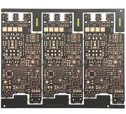
Multilayer PCB technology is widely used in modern electronic products that require high wiring density, compact dimensions, electrical performance, and reliable interlayer connections. Compared with single-sided and double-sided boards, a multilayer circuit board contains multiple conductive layers separated by dielectric materials and interconnected through plated holes and, where required, advanced via structures.
The manufacturing process of a Multilayer PCB involves multiple tightly controlled stages. These include inner-layer circuit fabrication, lamination, drilling, through-hole metallization, outer-layer circuit formation, solder mask application, surface finishing, profiling, electrical testing, inspection, and packaging.
A typical PCB Manufacturing flow can be summarized as:
Engineering and CAM Preparation → Material Cutting → Inner-Layer Circuit Fabrication → Lay-Up and Lamination → X-Ray Targeting → CNC Drilling → Desmear and Hole Metallization → Outer-Layer Circuit Formation → Solder Mask → Silkscreen → Surface Finish → Profiling → Testing → Final Inspection → Packaging
The exact process flow may vary depending on the board structure, layer count, materials, impedance requirements, HDI features, surface finish, and production specifications.
1. Engineering Preparation and Material Cutting
Before production begins, the manufacturing data is reviewed through engineering and CAM processes. Designers and manufacturing engineers verify the board outline, layer stackup, drill data, copper thickness, line width and spacing, impedance requirements, solder mask openings, surface finish, and other critical parameters.
For PCB Fabrication, the selected laminate system must be compatible with the electrical, thermal, mechanical, and reliability requirements of the application.
The copper-clad laminate is then cut into panels suitable for production. Material selection may include standard FR-4 systems as well as high-Tg, low-loss, high-frequency, halogen-free, or other specialty materials when required.
Proper material preparation is important because dimensional stability, dielectric properties, copper adhesion, and thermal performance directly influence subsequent manufacturing processes.
2. Inner-Layer Circuit Fabrication
The inner layers form the electrical foundation of a Multilayer PCB.
First, the copper surface is cleaned and conditioned to remove contamination and provide an appropriate surface for dry-film adhesion. Depending on the manufacturing process, brushing, chemical cleaning, or controlled micro-etching may be used.
A photosensitive dry film is then laminated onto the copper surface. The panel is exposed to ultraviolet light through the corresponding circuit artwork. During exposure, the appropriate areas of the photoresist are polymerized, transferring the circuit image onto the copper panel.
The exposed panel is developed using a suitable alkaline developer. Unwanted photoresist is removed, leaving the intended circuit pattern protected.
The exposed copper is then etched away using a controlled chemical process. After etching, the remaining dry film is stripped, revealing the completed inner-layer copper pattern.
At this stage, automated optical inspection (AOI) can be used to verify line width, spacing, opens, shorts, missing copper, and other pattern-related defe
3. Inner-Layer Surface Treatment and Inspection
Before lamination, the inner-layer copper surface needs to provide reliable adhesion to the dielectric material.
The copper surface may undergo controlled oxidation or alternative oxide-replacement/adhesion-enhancement treatment. The purpose is to improve the bonding interface between the copper circuitry and the resin system.
The inner layers are then inspected for:
- Circuit pattern accuracy
- Line width and spacing
- Copper defects
- Surface contamination
- Registration accuracy
- Open and short circuits
- Foreign particles and scratches
Good inner-layer quality is particularly important because defects become inaccessible after lamination.
4. PCB Lay-Up and Lamination
PCB Lamination is one of the most critical processes in multilayer board manufacturing.
The completed inner-layer circuits are combined with prepreg and copper foil according to the designed stackup. Prepreg acts as both an insulating dielectric and a bonding material between conductive layers.
The layer sequence must be carefully controlled to ensure correct electrical connections and dimensional registration.
During lay-up, manufacturing personnel or automated equipment align the inner layers, prepreg, copper foil, and tooling features. The stacked materials are placed between press plates and prepared for lamination.
The stack is then processed in a controlled lamination press. Temperature and pressure are applied according to the resin system and board construction. As the temperature increases, the resin softens and flows, filling appropriate spaces and bonding the layers together. The resin then cures and forms a mechanically stable multilayer structure.
Proper control of:
- Temperature profile
- Pressure
- Heating and cooling rates
- Resin flow
- Material thickness
- Layer registration
- Copper balance
is essential for reliable PCB Manufacturing.
Poor lamination control can contribute to delamination, resin starvation, voids, layer shift, warpage, and other reliability problems.
5. X-Ray Targeting and Registration
After lamination, the inner-layer circuits are enclosed inside the multilayer structure. Accurate alignment between the inner and outer layers is therefore essential.
X-ray equipment can be used to identify internal targets and establish accurate reference points for subsequent drilling and outer-layer processing.
The panel may also undergo edge trimming or other preparation steps before drilling.
Registration accuracy becomes increasingly important as line widths become smaller, layer counts increase, and advanced structures such as HDI microvias are introduced.
6. CNC Drilling
PCB Drilling creates the holes required for electrical interconnection, component mounting, mechanical positioning, and other functions.
CNC drilling machines use programmed drill data to produce through-holes and other required hole structures.
During drilling, the panel is accurately positioned using tooling or target features. Entry and backup materials may be used to help control burrs, surface damage, drill quality, and debris.
The drilling process must control parameters such as:
- Drill diameter
- Spindle speed
- Feed rate
- Tool wear
- Hole position
- Board thickness
- Aspect ratio
- Stack construction
For high-density boards, mechanical drilling may be combined with laser drilling to produce microvias or other fine interconnect structures when required by the design.
7. Desmear and Through-Hole Metallization
After drilling, resin smear can remain on the hole walls, particularly in multilayer structures where the drill passes through multiple resin and glass-fiber layers.
A desmear process removes or conditions unwanted resin residue and prepares the hole walls for metallization.
The panel then undergoes chemical conditioning and activation. A catalytic layer is created on the non-conductive hole wall so that electroless copper can be deposited.
During electroless copper plating, a thin conductive copper layer is deposited onto the hole walls. This establishes the initial electrical connection between the copper layers.
The panel can then undergo copper electroplating to increase the copper thickness in the holes and on the appropriate conductive surfaces.
This Through-Hole Plating process is essential for reliable interlayer electrical connectivity.
Copper thickness and plating uniformity must be carefully controlled because inadequate plating can reduce current-carrying capability and thermal reliability, while excessive or uneven plating can affect dimensional accuracy and downstream processing.
8. Outer-Layer Circuit Formation
After hole metallization, the outer-layer circuit is formed.
A photosensitive dry film is applied to the outer copper surface and exposed using the required circuit artwork. The panel is then developed to create the desired circuit pattern.
One common manufacturing approach is pattern plating. In this process, exposed conductive areas are selectively plated with copper and may receive an additional metallic etch-resist layer depending on the production flow.
After plating, the dry film is stripped. The exposed copper is then etched away while the protected circuit areas remain.
The etch-resist layer is subsequently removed when required, leaving the final outer-layer circuit pattern.
The process must maintain tight control of line width, spacing, copper thickness, registration, and surface condition.
9. Solder Mask Application
Solder mask provides protective insulation over most of the copper surface while leaving solderable pads, test points, and other designated areas exposed.
Modern PCB Fabrication commonly uses photosensitive solder mask materials. The solder mask is applied to the board surface and then exposed and developed to create precise openings.
The process normally includes:
- Surface preparation
- Solder mask coating
- Tack drying or preliminary curing
- UV exposure
- Development
- Final thermal curing
Solder mask helps reduce the risk of solder bridging during assembly and protects exposed copper from environmental contamination and oxidation.
Color selection, thickness, adhesion, registration, surface appearance, and curing conditions should all be controlled according to the application requirements.
10. Silkscreen and Marking
After solder mask processing, identifying information can be printed onto the board.
Silkscreen or other marking processes may include:
- Component reference designators
- Polarity indicators
- Connector labels
- Manufacturer information
- Revision information
- Product identification
- Warning or assembly markings
The marking must remain clear without interfering with solder pads, test points, or other functional areas.
11. PCB Surface Finish
After solder mask and marking, exposed copper pads require an appropriate PCB Surface Finish.
The surface finish protects exposed copper, improves solderability, and may provide the required contact characteristics for the intended application.
Common options include:
- HASL
- Lead-Free HASL
- ENIG
- Immersion Tin
- Immersion Silver
- OSP
- Electroplated Gold for specific contact applications
The appropriate finish depends on soldering requirements, pad geometry, storage conditions, contact durability, fine-pitch assembly, cost, and end-use environment.
For example, ENIG can provide a relatively flat surface suitable for fine-pitch components, while OSP offers a thin organic protective layer over copper. Gold plating for edge contacts has different requirements from immersion gold used as a solderable surface finish.
Therefore, surface finish selection should be based on the actual application rather than color or appearance alone.
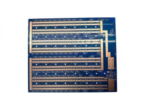
12. PCB Profiling and Final Machining
The finished panel is then separated into individual boards or customer-specified shapes.
Depending on the design, CNC routing, punching, V-scoring, or a combination of methods may be used.
PCB Manufacturing engineers must consider:
- Board dimensions
- Tolerances
- Cutout geometry
- Slots
- Mounting holes
- Edge connectors
- Panelization
- Depanelization requirements
For boards with gold fingers, the edge-contact area may require an appropriate beveling operation to facilitate connector insertion.
For panelized production, breakaway tabs, mouse bites, V-score lines, or other separation structures may be used according to the assembly and depanelization requirements.
13. Electrical Testing and Quality Control
Testing is an essential part of PCB Quality Control.
Depending on the product and customer requirements, manufacturers may use several inspection and testing methods.
Automated Optical Inspection
AOI checks visible circuit patterns for defects such as:
- Open circuits
- Shorts
- Missing copper
- Incorrect patterns
- Line-width abnormalities
- Solder mask registration issues
Electrical Testing
Electrical testing verifies connectivity and checks for unintended opens or shorts. Flying-probe or fixture-based testing may be selected according to production volume and board complexity.
Microsection Analysis
Microsection inspection can evaluate internal construction, including:
- Plated-hole copper thickness
- Layer registration
- Resin distribution
- Lamination quality
- Via structure
- Copper interfaces
Additional Reliability Testing
Depending on application requirements, additional testing may include thermal stress, solderability, insulation resistance, surface finish evaluation, impedance testing, or other qualification procedures.
14. Final Inspection and Packaging
Before shipment, completed boards undergo final visual inspection and dimensional verification.
Quality personnel may check:
- Board dimensions
- Surface appearance
- Solder mask condition
- Silkscreen clarity
- Surface finish
- Gold fingers or contact areas
- Hole quality
- Burrs and edge condition
- Contamination
- Packaging condition
Packaging must protect the boards from moisture, contamination, oxidation, mechanical damage, and electrostatic risks where applicable.
Common packaging methods include PE protective bags, moisture-barrier packaging, vacuum packaging, and other packaging configurations selected according to the board type and storage requirements.
Key Factors Affecting Multilayer PCB Manufacturing Quality
Producing a reliable Multilayer PCB requires coordination between design engineering, materials, fabrication processes, and inspection.
Several factors are especially important:
1. Stackup Design
The stackup affects impedance, signal integrity, power distribution, thermal behavior, and manufacturability.
2. Material Selection
Laminate selection should consider Tg, CTE, dielectric constant, dielectric loss, thermal conductivity, moisture behavior, and application requirements.
3. Registration Control
As board density increases, layer-to-layer registration becomes increasingly critical.
4. Drilling and Plating
Hole quality and plating reliability directly affect interlayer electrical connectivity.
5. Lamination Control
Resin flow, temperature, pressure, and material construction must be controlled to minimize delamination, voids, warpage, and layer shift.
6. Surface Finish
The selected PCB Surface Finish must be compatible with the assembly process, component pitch, storage environment, and product requirements.
7. Electrical and Visual Inspection
Inspection at different stages helps prevent defects from being carried into subsequent manufacturing processes.
Common Defects in Multilayer PCB Manufacturing
Typical defects may include:
- Layer misregistration
- Lamination voids
- Delamination
- Resin starvation
- Excessive resin flow
- Plated-hole voids
- Uneven copper plating
- Drill breakout
- Burrs
- Open circuits
- Short circuits
- Solder mask misregistration
- Surface finish defects
- Board warpage
Effective process control should focus not only on detecting defects but also on identifying their root causes.
Kingda’s Multilayer PCB Manufacturing Capabilities
For complex PCB Manufacturing projects, close coordination between PCB design and fabrication is essential.
Kingda can support customers through the manufacturing process, from engineering review and material selection to multilayer fabrication, drilling, plating, solder mask, PCB Surface Finish, testing, and final inspection.
For high-density and high-reliability applications, manufacturing considerations should be incorporated into the design at an early stage. DFM review can help identify potential problems related to line width, spacing, drill structures, stackup, registration, copper distribution, panelization, and assembly requirements before production begins.
Conclusion
The Multilayer PCB manufacturing process is a complex sequence of interconnected operations. Inner-layer circuit formation, PCB Lamination, PCB Drilling, Through-Hole Plating, outer-layer fabrication, solder mask, PCB Surface Finish, profiling, testing, and final inspection must work together to achieve consistent quality.
As electronic products become smaller and more integrated, multilayer boards increasingly require tighter registration, finer circuitry, advanced interconnect structures, improved signal integrity, and more sophisticated manufacturing controls.
Selecting an experienced manufacturing partner such as Kingda and involving the manufacturer early in the design process can help improve manufacturability, reliability, and production consistency.