Semiconductor Test Burn-in Board: The Complete Guide
What Is a Semiconductor Test Burn-in Board?
A semiconductor test burn-in board is a high reliability PCB that sits between a device under test and the burn-in oven or automatic test equipment used to qualify chips. Each board carries a number of test sockets, the chips are loaded into those sockets, and the whole assembly is powered and exercised for many hours while the oven holds the temperature at a demanding level. Because the board has to distribute power, carry test signals and stay dimensionally stable through hundreds of thermal cycles, it is built to much higher standards than an ordinary industrial PCB.
Burn-in boards are used to qualify AI processors, CPUs, GPUs, FPGAs, ASICs, DRAM, NAND flash, automotive microcontrollers and power semiconductors before they are shipped. The board itself rarely appears in the final product, yet its design and fabrication quality decide whether a weak chip is caught in the factory or fails in the field, which makes it one of the most reliability-critical PCBs manufactured today.
This guide explains how burn-in boards work, which materials and design rules keep them alive at high temperature, how they are manufactured, what quality standards apply and what they cost in 2026.
Why Chips Need Burn-in Testing
Even after packaging, a chip can carry hidden defects: wafer fabrication anomalies, marginal wire bonds, encapsulation stress, weak solder joints, electrostatic damage or material degradation. Most of these flaws only show themselves after the device has run hot and hard for a while, which is why high reliability chips are screened before delivery.
During burn-in the devices are held at junction temperatures in the 125 to 175 degree Celsius range while biased and loaded continuously for tens to hundreds of hours. The accelerated stress pushes weak parts to fail early, so the customer receives a population that has already survived the infant mortality period. Without this screening, failures appear later as system crashes, data loss, vehicle electronics faults, industrial downtime or medical equipment failure, at a cost far above the price of a test board.
How a Burn-in Board Works
The workflow is simple in concept and demanding in execution. Chips are mounted into test sockets, the sockets are fixed to the burn-in board, and the board connects to the burn-in system. The oven rises to the programmed temperature, the system applies supply voltages and clock and pattern programs, and current, voltage and functional status are monitored automatically. Devices that drift outside the specification are flagged and logged, and the survivors move on to the next test stage.
Throughout that process the PCB must hold controlled impedance, keep signal loss low and move heat out of the socket area. Any drift in the board under heat corrupts the test result, so impedance stability, low loss materials and a well planned thermal path are not optional features; they are what make the measurement trustworthy.
Main Types of Burn-in Boards
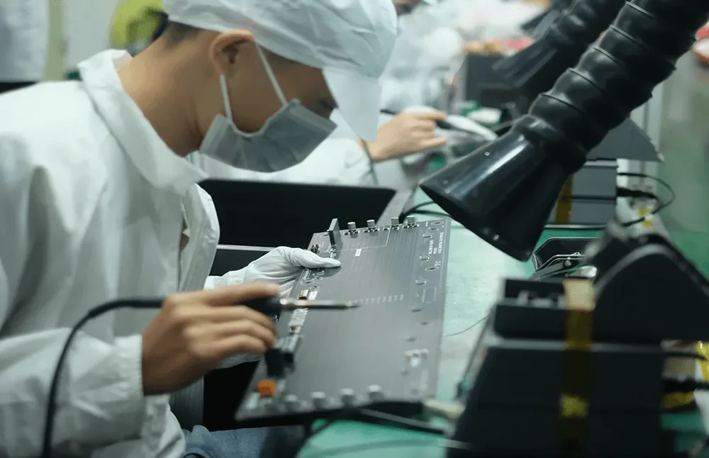
Because every package family has different contact and routing needs, burn-in boards are specialized by device type. BGA burn-in boards serve ball grid array packages with dense routing and tight impedance control for CPUs, GPUs and AI accelerators. QFN boards are built for automotive, industrial and consumer devices in quad flat no lead packages. CSP boards support chip scale packages with very fine pitch traces.
Flip chip boards handle high speed, high frequency, high power devices and therefore demand excellent thermal performance and signal integrity. Memory boards qualify DDR, LPDDR, HBM and NAND parts and are among the most channel-dense designs produced. AI processor boards push the limits hardest, often combining very high layer counts, thick copper and sophisticated heat spreading structures in one panel.
PCB Materials That Survive the Oven
Material choice dominates burn-in board reliability because the laminate must tolerate sustained heat, match the thermal expansion of the system and keep its electrical properties stable. High Tg FR-4 is the economical baseline for routine temperature testing; it is mature, inexpensive and stable enough for many applications. Polyimide laminates step up for long term high temperature operation thanks to superior heat resistance, low thermal expansion and strong resistance to thermal shock.
Rogers and other low loss high frequency materials are specified where high speed interfaces must keep impedance and low loss behavior at temperature. High CTI laminates improve insulation reliability in high voltage test environments, and ceramic boards are chosen for extreme temperature or very high power applications where their high thermal conductivity and dimensional stability win. Choosing the right material against the real test profile is usually the single biggest reliability decision on the board.
Design Rules for High Temperature Reliability
Burn-in board layout balances electrical performance, thermal management and mechanical survival. The stack-up must tolerate operating temperatures above 150 degrees Celsius without delamination or blistering, which drives resin system selection and lamination quality. High speed interfaces need controlled impedance and matched differential pairs, with complete return paths and minimized crosstalk, so test data stays accurate.
Heat management relies on thicker copper foils, thermal vias, large copper areas, copper coin inserts and metal heat sinks to pull heat away from the sockets. Power integrity design, clean grounding and low inductance supply paths keep voltage accurate while many devices switch at once. Because sockets are inserted and removed repeatedly, pad finish and durability must survive thousands of contact cycles. Finally, copper balancing and a symmetric stack-up limit warpage, which would otherwise break contact during thermal cycling.
Manufacturing Process and Surface Finish
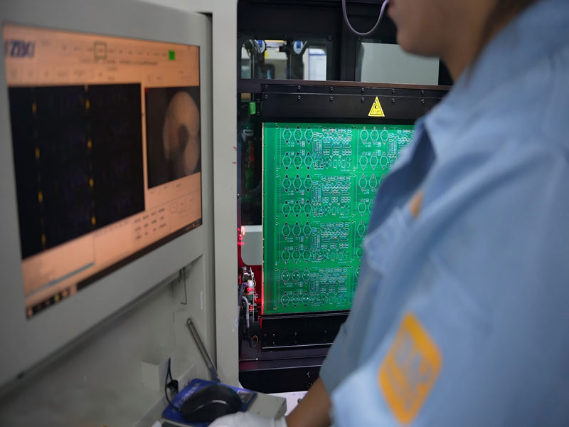
Building a burn-in board follows a controlled sequence: engineering review and DFM analysis, material verification, multilayer lamination, CNC drilling, laser microvia processing where HDI layers are present, through hole plating, imaging, surface finish and final inspection with AOI, electrical test, dimensional check and reliability verification. Capability requirements are demanding: very high layer counts, fine lines and spaces, tight hole registration, controlled impedance, low warpage processing and consistent copper thickness.
Surface finish matters more here than on almost any other board type because the finish is what survives repeated socket contact. ENIG offers flat, oxidation resistant, solderable pads and suits most programs. Hard gold provides excellent wear resistance and stable contact resistance for high frequency insertion cycles. ENEPIG combines the best of both worlds with excellent wire bond performance and contact reliability for advanced packaging and premium semiconductor test programs.
IPC Standards and Quality Requirements
Serious burn-in board programs are manufactured to IPC-6012 Class 2 or Class 3, with workmanship judged against IPC-A-600, design guidance from IPC-2221, laminate specifications from IPC-4101 and test methods from IPC-TM-650. Environmental compliance covers RoHS and REACH, and the facility should operate under an ISO 9001 quality system. These standards control dimensional accuracy, electrical performance and long term reliability, and they give the test lab a defensible paper trail for its qualification data.
Common Failure Modes and How to Prevent Them
When design or process control slips, burn-in boards fail in recognizable ways: warpage under thermal cycling, layer separation, pad lift, copper fatigue, high temperature oxidation, intermittent socket contact, signal attenuation and thermal cracks. Nearly all of these can be traced back to material mismatches, unbalanced copper, poor via design or inadequate lamination. A thorough DFM review at the design stage, realistic material selection and a manufacturer with high temperature experience reduce the risk dramatically before the first panel is built.
Typical Applications
Burn-in boards are deployed wherever silicon reliability is non-negotiable: AI server processors, GPU accelerators, CPUs and data center chips, autonomous driving processors and automotive ECUs, industrial controllers, medical electronics, aerospace systems, 5G equipment, power devices and new energy vehicle control systems. As advanced packaging and high performance computing grow, the demand for stable, high precision burn-in test PCBs keeps increasing.
2026 Price Reference for Burn-in Boards
Pricing depends on layer count, laminate, board size, impedance control, finish, copper weight and batch size. As a 2026 reference, prototype quantities of one to five boards typically run between 250 and 900 US dollars per board. Small batches of ten to fifty boards usually fall to 180 to 550 dollars per board, and medium volumes of one hundred to five hundred boards can reach 90 to 280 dollars per board. Production quantities are quoted against the actual design, because the difference between a simple high Tg FR-4 stack and a thick copper polyimide or Rogers build is large.
The main cost drivers are high Tg or polyimide laminates, Rogers or ceramic substrates, HDI and blind buried via structures, controlled impedance, thick copper from two to six ounces and beyond, ENEPIG or hard gold finish and the reliability testing required on top. Early DFM optimization removes unnecessary process steps and usually brings the per-board cost down without touching quality.
Choosing a Burn-in Board Manufacturer
The supplier matters because burn-in boards reward experience in high layer counts and extreme materials. Look for a factory that supports more than sixty layer multilayer boards, works routinely with high Tg, polyimide, Rogers and ceramic materials, holds tight impedance tolerances, processes HDI and laser microvias, and can plate copper to ten ounces where thermal designs need it. Full electrical test, AOI, X-ray and reliability verification should be standard rather than special requests.
gopcb manufactures high reliability multilayer PCBs for semiconductor test, automotive, medical and industrial programs, with engineering DFM support, IPC Class 2 and Class 3 production, ENIG, ENEPIG and hard gold finishes, and PCB testing services that match the demands of burn-in hardware. Send your Gerber files, stack-up, material requirements and test profile for a free DFM review and a quotation from prototype through production volume.