PCB Size: Standards, Thickness, Tolerances and Cost Guide
What PCB Size Really Covers
PCB size is more than the length and width printed on a drawing. It includes every mechanical dimension that determines whether a board can be fabricated, assembled and installed: overall outline, board thickness, copper weight, drilled hole sizes, via dimensions, profile tolerances and the edge clearance that keeps copper away from the board boundary. Each of these parameters interacts with the manufacturing process, so a dimension that looks harmless on paper can become a yield killer on the production floor.
Size decisions shape electrical behavior as well as mechanical fit. They influence signal integrity, EMI performance, heat spreading and mechanical strength, and they set the cost of the board because material consumption, drilling time and process complexity all scale with physical size. Engineers who treat PCB size as a first class design input rather than an afterthought get boards that are cheaper, more reliable and easier to assemble.
This guide covers common board sizes, standard thickness values, copper weights, tolerances, hole and via sizes, edge clearance rules, IPC guidance and the relationship between size and price.
Common PCB Sizes by Application
There is no single IPC standard size that every board must follow, and real products use whatever geometry their enclosure demands. That said, application patterns are recognizable. Small boards around 20 by 20 millimeters, 50 by 50 millimeters or 100 by 100 millimeters serve wearables, IoT terminals, Bluetooth modules and consumer devices. Medium boards such as 150 by 100 millimeters and 200 by 150 millimeters cover industrial control, power modules, communications gear and instruments.
Large boards at 300 by 250 millimeters and 500 by 400 millimeters appear in industrial automation, base stations, medical equipment and network switches, while very large formats run in AI server backplanes, data center equipment and aerospace or defense electronics. Capable factories routinely process panels up to 1200 by 650 millimeters, and sometimes larger for special programs.
Standard PCB Thickness Values
Board thickness is the dimension buyers quote most often. The industry default is 1.6 millimeters, which matches the historical 0.062 inch standard; it is the cheapest and most mature option, offers good mechanical strength and works with standard SMT assembly. The common catalog of thicknesses runs from 0.2, 0.4, 0.6 and 0.8 millimeters up through 1.0, 1.2, 1.6, 2.0, 2.4 and 3.2 millimeters.
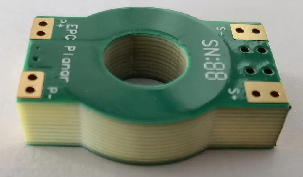
Ultra-thin boards between 0.1 and 0.4 millimeters serve flexible electronics, medical devices, smart cards and camera modules, while thick boards from 2.4 to 6.0 millimeters and beyond handle high power supplies, solar inverters, energy storage, motor drives and heavy industrial equipment. Choosing a catalog thickness whenever possible keeps cost and lead time down, because non-standard thicknesses often require special material procurement.
How Copper Weight Relates to Board Size
Copper weight is part of the size conversation because it changes the electrical and thermal design envelope. Half-ounce copper, around 17 micrometers, suits dense, small format electronics. One ounce, about 35 micrometers, is the standard for over ninety-five percent of boards. Two ounce copper, roughly 70 micrometers, serves LED lighting, industrial controls, power boards and battery management systems, and heavy copper from three to twenty ounces is used in new energy vehicles, high current equipment, UPS systems and photovoltaic storage.
Thicker copper constrains how fine traces can be etched and how small holes can be drilled, so a large high current board with heavy copper needs different design rules than a small signal board. The right approach is to size the copper from the current and thermal requirement, not from habit.
PCB Size Tolerances Explained
No PCB is manufactured with zero error, because material shrinkage, drilling and lamination all introduce small deviations. Standard outline tolerance is plus or minus 0.10 millimeter, with precision profiling reaching plus or minus 0.05 millimeter. Thickness is usually controlled to plus or minus ten percent, so a 1.6 millimeter board may measure between 1.44 and 1.76 millimeters.
Hole tolerances depend on the process: mechanical drilling holds roughly plus or minus 0.075 millimeter, while laser drilling reaches plus or minus 0.025 millimeter. Copper thickness is generally controlled to plus or minus ten percent. Automotive, medical and high speed programs demand the tighter end of every range, which is why their fabrication costs more than commodity boards.
Hole and Via Sizes
Drilled features dominate the relationship between board size and density. Common through hole diameters run from 0.20 to 1.00 millimeter, with ordinary vias drilled at 0.20 to 0.30 millimeter and pad diameters of 0.45 to 0.60 millimeter. Microvias for HDI boards are laser drilled at 0.075 to 0.15 millimeter and appear in smartphone main boards, AI servers and high speed communications equipment.
Hole size selection interacts with board thickness through the aspect ratio: thick boards limit how small a through hole can be reliably plated. Designers who keep the via diameter and the board thickness inside the manufacturer’s capability window avoid plating voids and barrel cracks.

Edge Clearance Requirements
Edge clearance is the distance between copper features and the board edge, and it exists to protect the board during routing and in service. For ordinary boards the recommended minimum is 0.5 millimeter, with 0.25 millimeter accepted on dense designs. High voltage boards need far larger spacing based on working voltage, sometimes 2, 4 or more millimeters, to guarantee insulation and safety.
Insufficient edge clearance causes electrical breakdown, delamination, edge chipping during profiling and SMT placement problems. Good panelization and adequate clearance keep the profile operation clean and the finished edge durable.
IPC Standards That Govern Board Size
The IPC framework controls how board dimensions are designed, inspected and accepted. IPC-A-600 defines appearance and acceptance criteria, IPC-2221 provides general PCB design rules, IPC-6012 covers rigid board performance, IPC-6013 covers flexible boards and IPC-6018 applies to high frequency boards. Manufacturing to these standards satisfies international OEM purchasing requirements and keeps quality consistent from batch to batch.
How PCB Size Drives Cost
Size is one of the largest levers on price. Larger boards consume more laminate, require more drilling and take longer to process, so material and labor rise with area. Thicker boards need more prepreg and lamination cycles. Tight tolerances add inspection time and lower yield, and HDI or microvia designs add laser drilling, multiple lamination passes and precise registration, all of which multiply cost.
Because panel utilization is the hidden factor, an odd board shape that wastes panel area can cost far more than its outline suggests. Reconsidering the profile or panelization layout is frequently the cheapest way to reduce price without changing the circuit.
DFM Advice for Board Dimensions
Good dimensioning starts with standard values. Prefer catalog thicknesses such as 0.8, 1.0 or 1.6 millimeters, avoid tight tolerances on non-critical features, and plan the panel layout so utilization stays high. Keep edge clearance generous, follow IPC design guidance, and run a DFM review with the factory before release. Those habits prevent the dimension related changes that slow prototypes and inflate cost.
2026 Price Reference by Board Class
As a 2026 reference, a two layer FR-4 prototype of 100 by 100 millimeters in quantities of five to ten boards typically costs 5 to 30 US dollars. In small batch production of one hundred to five hundred boards, a four layer board commonly lands between 0.8 and 8 dollars per board. Above ten thousand boards, four to eight layer boards can reach 0.10 to 3 dollars per board. HDI boards range widely from 20 to 300 dollars per board depending on layer count, microvia density and complexity.
Actual pricing depends on the Gerber data and the BOM, which is why a DFM analysis against real manufacturing capability is the fastest route to an accurate quotation.
FAQ
Is there a standard PCB size? No single size is mandated. Applications follow common ranges, and the factory can process boards from small module formats up to 1200 by 650 millimeters or larger.
What is the most common PCB thickness? 1.6 millimeters is the default because it balances cost, strength and SMT compatibility, with 0.8 and 1.0 millimeter also widely used.
Does a bigger board always cost more? Generally yes, because material, drilling and processing scale with area, but panel utilization can matter more than raw size, so an awkward outline may cost more than a larger efficient one.
Manufacturing Boards of Any Size Correctly
Board size is only a problem when the factory cannot handle it. Choose a partner with wide capability so dimension questions never become capability questions. gopcb manufactures from 1 to 80 layers with maximum board sizes of 1200 by 650 millimeters, thickness from 0.1 to 10 millimeters, minimum mechanical drills of 0.15 millimeter, laser microvias of 0.075 millimeter and copper from 0.5 to 20 ounces under IPC Class 2 and Class 3 programs. For PCB manufacturing and assembly support, send your outline and stack-up files for a free DFM review and a size-accurate quotation.