Flex PCB Outline: Design Rules, Cutting Methods and Cost
What Is a Flex PCB Outline?
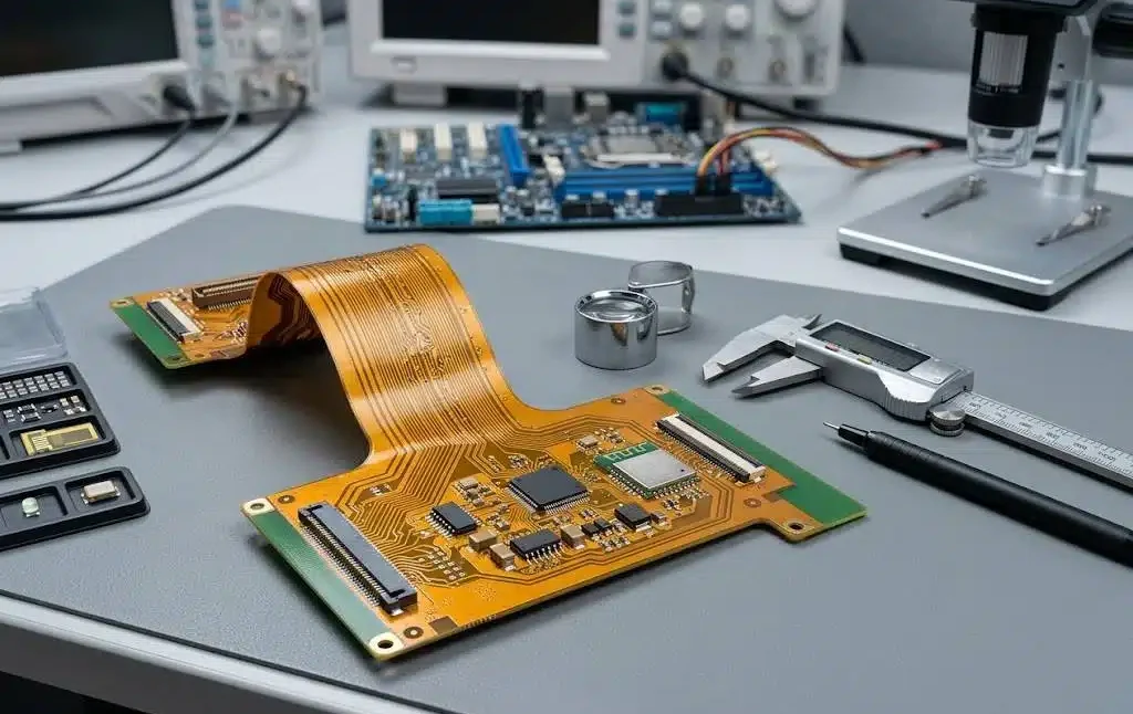
The flex PCB outline is the mechanical profile that defines the final shape of a flexible circuit: the outer contour, internal windows, slots, mounting and tooling holes, connector areas, stiffener locations and the rounded corners that keep the material from tearing. Unlike rigid boards, flex circuits are thin and mechanically delicate, so the outline is not a cosmetic detail; it decides whether the part can be profiled cleanly, assembled accurately and bent reliably for its whole service life.
A complete outline definition includes the outer boundary, cutouts and slots, breakaway tabs for panelization, gold finger regions, stiffener pads, fiducials and the copper clearances around every edge feature. Every one of those elements must be designed with the cutting process in mind, because a contour that works beautifully for one factory may be impossible for another.
This guide covers the cutting methods used for flex circuits, the design rules that protect the material, tolerances, IPC standards and realistic costs.
Why the Outline Matters More on Flex Boards
Flexible laminates have low mechanical strength, so poorly designed outlines fail in recognizable ways: copper tears at sharp corners, material rips during depanelization, profiles shift out of tolerance, and repeated bending cracks traces near the edge. Good outline design prevents those failures before they start.
A well planned profile also raises manufacturing yield, improves assembly accuracy for connectors and stiffeners, extends bending life by removing stress concentrators, and gives consumer products the clean, consistent edge quality customers expect. In other words, the outline directly influences yield, reliability and appearance at the same time.
Cutting Methods for Flex PCB Outlines
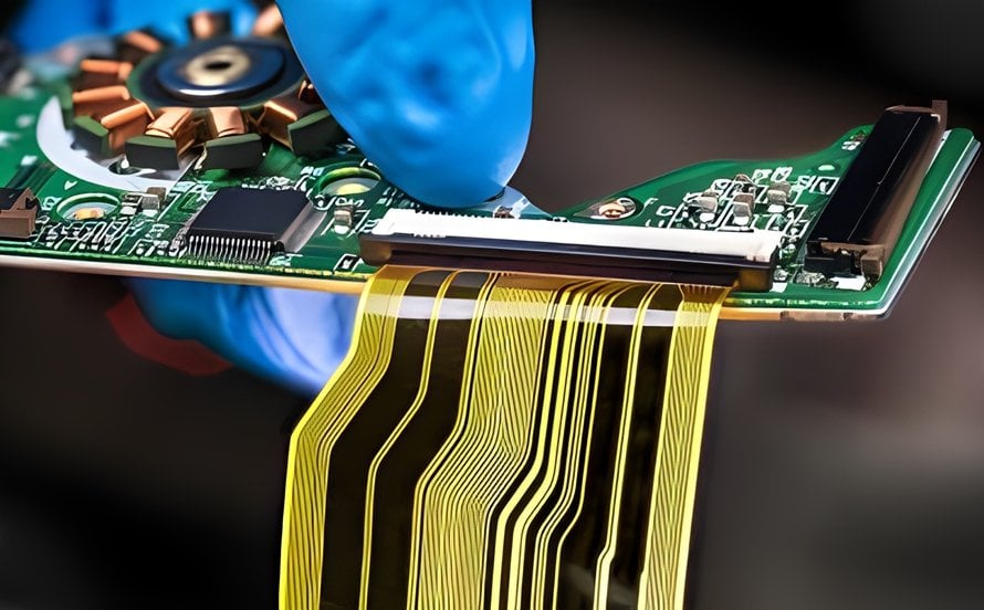
Laser cutting is the most accurate profiling method for flex circuits, typically reaching plus or minus 0.05 millimeter. It handles complex contours and internal windows without mechanical stress, needs no tooling, and is ideal for medical, wearable, smartphone, camera module and high density flex prototypes and small batches.
Die cutting is the workhorse of high volume flex production: the per-part cost is lowest, speed is high and dimensional consistency is excellent, but tooling must be made up front and every design change requires a new die. Typical tolerance is plus or minus 0.10 millimeter. CNC routing offers a middle path with no tooling, flexible scheduling and good edge quality at about plus or minus 0.10 millimeter for medium batches and frequent design iterations, while punching suits simple, extremely high volume parts.
Design Rules That Protect the Material
The most important rule is to avoid sharp ninety degree corners. Internal corners should use radius transitions so stress spreads instead of concentrating, which dramatically improves flex endurance. Copper should stay well away from the edge: at least 0.20 millimeter for standard products and 0.30 millimeter or more for high reliability builds, otherwise the copper can lift or crack during profiling.
Keep breakaway tabs wide enough to survive production, handling and depanelization. Avoid placing vias in bending zones, and position stiffeners, mounting holes and fiducials with generous tolerances so connectors and pads align correctly in the final assembly. Adding stress relief slots around bend lines and designing the bend radius against the material thickness prevents the trace fatigue that ends the life of a flex circuit prematurely.
Typical Tolerances by Process
Tolerance expectations follow the process. Laser cutting holds about plus or minus 0.05 millimeter on the profile; CNC routing and die cutting both land near plus or minus 0.10 millimeter. Hole position accuracy is typically plus or minus 0.05 millimeter and stiffener placement about plus or minus 0.10 millimeter. Medical optics, aerospace and other high precision programs can tighten these values further when the design and the process are matched.
Common Flex Outline Features
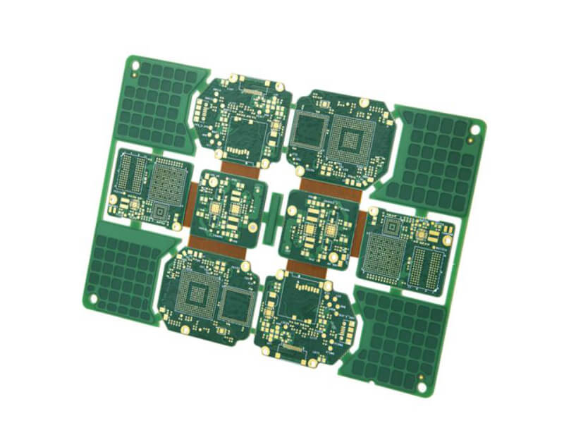
Production flex boards combine many mechanical features in one profile: dynamic bending zones, gold fingers, stiffeners, EMI shielding areas, locating holes, panel rails, half-cut structures, tear bridges and heat windows. Each feature interacts with the cutting process. Deep slots need enough material around them, gold fingers need accurate registration with the plating step, and stiffener areas need clearance for the adhesive that bonds them. All of these should be reviewed against the factory’s tooling before the files are released.
Choosing the Right Profiling Process
Process selection is an economic decision as much as a technical one. Laser cutting wins when precision, complexity or small quantities are involved, and it is the standard for medical and consumer electronics prototypes. Die cutting wins at scale: the tooling investment pays off when annual volume is high and the design is stable. CNC routing suits medium volumes and projects where the outline still changes between batches. Match the process to the product lifecycle and the tooling cost disappears into the unit price.
DFM Review Points for Flex Outlines
Before production, review the outline for the failure modes that matter: copper to edge spacing, corner radii, tab widths, via placement versus bending zones, stiffener sizes and locations, connector mechanical dimensions, panel utilization, tooling holes and fiducials, and consistency between the Gerber mechanical layers, drill layers and the DXF source file. Catching these points in review avoids rework, shortens lead time and raises yield on every batch.
IPC Standards for Flex Circuit Outlines
Flexible circuit design and acceptance follow a dedicated standard set. IPC-2223 covers flex PCB design, IPC-6013 defines flex performance and acceptance, IPC-A-600 governs appearance acceptance and IPC-A-610 covers electronic assembly acceptance. Manufacturing to these standards keeps dimension control, mechanical reliability and long term stability consistent across suppliers and batches.
2026 Cost Reference for Flex Profiling
Profiling cost depends on size, layer count, material, process, tolerance and quantity. As a 2026 reference, flex prototypes of one to twenty pieces typically run 50 to 200 US dollars for the full board service, covering design verification and functional testing. Small batches of fifty to five hundred boards usually cost 2 to 15 dollars per board depending on laser profiling, stiffener count and outline complexity. Above one thousand boards, die cutting and optimized panelization typically bring the price down to 1 to 5 dollars per board.
The cheapest cost lever is the same as the quality lever: an outline designed for the process, with high material utilization and no over-specification.
FAQ
Which process gives the most accurate flex outline? Laser cutting, at about plus or minus 0.05 millimeter, which is why complex and high reliability flex boards use it.
How much copper clearance is needed at the edge? At least 0.20 millimeter for standard products and 0.30 millimeter or more for high reliability designs.
Can flex boards have complex shapes and internal windows? Yes. Laser cutting and CNC routing both handle complex contours, internal windows, slots and special mechanical features.
Profiling Flex Boards With the Right Partner
Flex outline work rewards manufacturers with real process depth. Choose a factory that runs single, double and multilayer flex as well as rigid-flex, owns laser cutting, CNC routing and die cutting capability, laminates FR4, polyimide and stainless stiffeners, and manages finish, assembly and test under IPC Class 2 and Class 3 programs. gopcb offers flexible PCB manufacturing with high precision outline processing, DFM engineering review and prototype through high volume delivery. Send your Gerber, DXF or mechanical drawings for a free outline review and quotation.