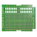
78 Layer Orthogonal Backplane PCB: Structure, Materials and Applications
Why the Industry Is Moving to Orthogonal Backplanes
AI training, high performance computing, cloud data centers and next generation communication networks keep raising the bar for high speed interconnect. Traditional backplanes struggle when they must carry 112G PAM4, 224G PAM4 and future 400G-class signals because signal loss, crosstalk and thermal limits grow quickly at those rates. To solve the problem, high end equipment is moving to the orthogonal backplane architecture, and the 78 layer orthogonal backplane PCB represents one of the most advanced capabilities in high layer count board manufacturing today.
This guide explains what a 78 layer orthogonal backplane PCB is, how the architecture works, which stack-ups and materials are used, how signal integrity and manufacturing are controlled, where these boards are applied and what they cost in 2026.
gopcb builds advanced high layer count boards through its PCB manufacturing service.
What Is a 78 Layer Orthogonal Backplane PCB?
A 78 layer orthogonal backplane PCB is an ultra large multilayer board that connects the functional cards of a high end electronic system. Unlike a traditional parallel backplane, the orthogonal design places line cards and fabric cards at 90 degrees to each other, which shortens the signal path and improves electrical performance.
Its main characteristics include 78 or more layers, support for 112G and 224G PAM4 transmission, very large panel sizes, ultra low loss materials, strict impedance control and high reliability requirements. Typical parameters are 60 to 80-plus layers, board thickness from 10 mm to 18 mm, maximum size around 800 mm by 600 mm, differential impedance of 85 or 100 ohm, and data rates from 56G through 224G PAM4.
How the Orthogonal Architecture Works
In a traditional backplane, every line card plugs in parallel, which creates long signal paths, higher insertion loss, more crosstalk and restricted airflow. The orthogonal architecture places the line card and fabric card at 90 degrees so signals travel straight through the shortest possible interconnect.
That brings four major benefits. Signal paths are shorter, so high speed attenuation drops. System bandwidth increases, supporting 400G, 800G and even 1.6T Ethernet links. Cooling improves because the layout forms cleaner airflow paths between cards. Routing density rises, allowing far more high speed channels on one board.
Typical Structure of a 78 Layer Board
A 78 layer PCB uses a complex, highly symmetrical stack-up to control warpage. About 30 to 40 layers are signal layers carrying high speed differential pairs, SerDes channels and the fabric switching network. About 20 to 25 layers are ground layers that provide return paths, suppress EMI and strengthen signal integrity. About 10 to 15 layers are power layers for core voltages, high current distribution and power integrity optimization, and additional shielding layers isolate high speed signals and cut crosstalk. The entire stack is designed symmetrically so that copper balance keeps the panel flat through lamination.
Materials for Ultra High Layer Orthogonal Backplanes
Material performance decides transmission quality at 112G and 224G. Panasonic Megtron 6 is one of the most common choices for AI servers and 800G switches because of its very low loss, good dimensional stability and high reliability. Tachyon 100G targets high speed communication with extremely low dissipation factor and ultra low insertion loss for core routers and telecom switches. Isola I-Speed balances performance and cost for enterprise and industrial network equipment.
Key material targets are a dielectric constant around 3.0 to 3.5, a dissipation factor of 0.005 or lower, and a glass transition temperature of 180 degrees Celsius or higher. These values keep the board capable of the low loss and dimensional stability that 112G-plus channels demand.

Signal Integrity Design
Signal integrity is what separates a working orthogonal backplane from an expensive failure. Differential impedance is normally held at 85 or 100 ohm with a tolerance around plus or minus 5 percent, and insertion loss on critical channels should stay below about 28 dB at the Nyquist frequency.
Crosstalk is controlled by increasing line spacing, adding ground layers and using orthogonal routing patterns. Back drilling removes via stubs that would reflect high speed energy, making the process almost standard for 112G and 224G systems. SI simulation should happen before fabrication to verify insertion loss, return loss, crosstalk and eye diagram margin, because changes after tooling are extremely expensive on a 78 layer product.
Manufacturing Challenges
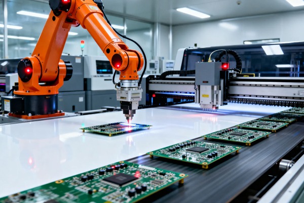
Producing a 78 layer orthogonal backplane demands exceptional registration accuracy, multiple precise lamination cycles and very large process equipment because many backplanes exceed 600 mm in one dimension. Copper balance and symmetrical stack-ups are mandatory to control warpage on thick, oversized panels. High speed laminates also need careful handling because the materials are more sensitive to moisture and process temperature than standard FR-4.
Quality control follows IPC-6012 Class 3 for high reliability boards, with IPC-A-600 appearance, IPC-2221 design and IPC-4101 material standards as reference. Boards are checked with AOI, X-ray, flying probe, cross sectioning, thermal stress and IST reliability testing before shipment, supported by the same discipline used in gopcb’s PCBA testing services.
Main Applications
78 layer orthogonal backplanes serve the most demanding systems in the industry. AI servers use them in GPU servers, training clusters and inference platforms. Hyperscale data centers rely on them for 800G switches and spine leaf architectures. Communication equipment such as core routers, telecom switches and optical transport systems uses the architecture for its short, clean signal paths, and supercomputers depend on it for scientific computing and national HPC centers.
DFM Advice Before You Order
To keep yield high, the stack-up must stay symmetrical, via structures should use back drilling, via shielding and stub free design, and copper should be balanced across every layer so no large copper area sits alone. Material lead times matter: ultra low loss laminates can take weeks to source, so the material plan should be confirmed early. Finally, run SI simulation before release, including loss, return loss, crosstalk and eye margin checks, to avoid expensive rework.
2026 Cost Reference
A 78 layer orthogonal backplane is one of the most expensive products in the PCB industry because of its layer count, size and exotic materials. Prototypes of 1 to 5 pieces typically cost 8000 to 20000 USD per board. Small batches of 10 to 50 pieces run about 5000 to 12000 USD per board, and medium batches of 50 to 200 pieces fall to roughly 3000 to 8000 USD per board.
Price is driven by layer count, laminate brand and loss grade, board thickness, number of back drilled holes, impedance requirements, testing scope and IPC class. An early PCB design and layout review and material commitment protects both schedule and budget on such a long lead time product.
FAQ
Where are 78 layer orthogonal backplanes used? AI servers, hyperscale data centers, telecom switches, core routers, aerospace and supercomputers are the main applications.
Why is an orthogonal backplane better than a traditional one? The 90 degree card layout shortens signal paths, which cuts insertion loss and crosstalk while improving airflow and system bandwidth.
Does a 78 layer PCB need back drilling? For 112G and 224G systems, back drilling is almost standard because it removes via stubs that cause signal reflection.
Which materials suit 78 layer high speed backplanes? Megtron 6, Tachyon 100G and Isola I-Speed are common choices with low loss and high reliability.
How long does 78 layer orthogonal backplane production take? Prototypes normally need 6 to 10 weeks and production 8 to 14 weeks, depending on material procurement and process complexity.
Get an Orthogonal Backplane PCB Quote
AI model training, 800G switching and future 1.6T interconnect are making the orthogonal backplane architecture essential for next generation systems, and its design, materials and signal integrity control represent the top tier of PCB technology. gopcb offers Megtron and Tachyon material processing, high precision back drilling, oversized backplane production, strict impedance control and IPC Class 3 quality with AOI, X-ray, flying probe and cross section verification. Send your stack-up and Gerber files for a free DFM review and an orthogonal backplane PCB cost estimate.