Attendance System PCB: Design, Manufacturing and OEM Guide
Why the Attendance System PCB Matters
Digital offices, smart campuses, smart factories and intelligent access control are changing the way attendance is recorded. Traditional card punching has been replaced by systems that combine RFID, fingerprint, face recognition, NFC, QR codes, cloud management and AI algorithms. Whether it is an employee time clock, a school attendance terminal, a visitor device or an access control unit, the core hardware always depends on a reliable attendance system PCB.
For device manufacturers, a stable board decides machine performance, product life, maintenance cost and market competitiveness. This guide explains the design requirements, manufacturing process, PCBA assembly, quality control, cost reference and OEM solutions for attendance system PCBs, helping engineers, buyers and product teams understand the complete production flow.
gopcb offers complete fabrication and assembly support through its PCB manufacturing and turnkey PCB assembly services.
What Is an Attendance System PCB?
An attendance system PCB is the core circuit board inside a smart attendance device. It connects, controls and coordinates the functional modules of the terminal, which typically include an MCU or ARM controller, RFID reader, NFC module, fingerprint sensor, face recognition camera, infrared fill light, LCD or touch display, Wi-Fi, Bluetooth, Ethernet, USB, real time clock, flash memory, power management, buzzer and voice circuits, and relay outputs for door locks.
Because AI algorithms and edge computing now run inside the terminal, modern attendance equipment often uses four to ten layer boards or even HDI designs to support high speed data, high reliability and dense interfaces in one compact product.
Attendance Device Types and Their PCB Needs
RFID card attendance systems are widely used in offices, schools, hospitals and factories. They typically need two to four layer FR-4 boards with one ounce copper, an integrated RFID antenna, EMI optimization, low cost and high stability.
Fingerprint attendance systems demand more processing power. The board carries the fingerprint sensor, a high performance MCU, flash, a security encryption chip and USB, so four to six layers with power integrity, controlled impedance and good EMC performance are recommended.
Face recognition systems are AI vision products that integrate an AI processor, RGB and infrared cameras, fill lights, a high resolution display, Wi-Fi, Bluetooth and gigabit Ethernet. These products use six to ten layer HDI boards with high speed differential routing, blind and buried vias and EMI shielding.
All in one smart attendance terminals support face, fingerprint, RFID, NFC, QR code, GPS and 4G or 5G connectivity in a single unit, which raises the requirement to HDI high density interconnect with strict manufacturing and assembly control.
Key Design Points for Attendance Boards
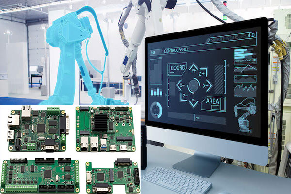
Signal integrity. Modern attendance terminals contain USB, DDR, MIPI camera, Ethernet and LCD interfaces. High speed nets need differential impedance control, matched length routing, continuous reference planes and fewer via transitions to reduce crosstalk and reflection.
Power integrity. The system uses 12V, 5V, 3.3V, 1.8V and 1.2V rails. A complete power plane, optimized decoupling and wide copper traces keep the supply stable while the camera, wireless modules and display draw bursts of current.
EMC and EMI design. Attendance devices run in offices and industrial environments for years. Large ground areas, via stitching, optimized return paths, power filtering, ESD protection on interfaces and RF module isolation help the product pass certification.
Thermal management. AI processors, communication modules and display drivers generate heat. Thermal vias, large copper areas, thicker copper, heatsinks and thermal pads keep junction temperatures low and extend product life.
Materials and Surface Finish
FR-4 is the most common substrate for attendance boards because it balances cost and reliability. High Tg FR-4 suits industrial environments where the terminal runs at higher ambient temperature, and high speed materials such as Megtron, Isola and Rogers families are reserved for AI attendance terminals with fast processors and camera interfaces.
ENIG is the recommended finish for most attendance devices because it offers flat pads, excellent solderability, corrosion resistance and long term reliability, especially on boards with fine pitch BGAs and cameras.
Manufacturing and Assembly Flow
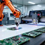
Production starts with front end engineering and DFM review, then material preparation, inner layer imaging, lamination, drilling, plating, outer layer imaging, solder mask, finish, electrical test and inspection. The bare board then enters PCBA where SMT placement, through hole insertion, programming, functional test and, when requested, conformal coating are performed. Turnkey sourcing means the manufacturer buys components and manages the BOM, which shortens lead time for OEM customers.
Because attendance devices combine analog sensing, digital processing and wireless communication, assembly quality directly affects antenna performance, camera image stability and long term reliability. A single quality system from board to box build reduces the risk of defects slipping between suppliers.
Quality Control and Standards
Boards are verified with AOI, X-ray, flying probe and functional test before delivery. IPC Class 2 is typical for commercial attendance products while Class 3 applies to high reliability or medical grade terminals. IPC-A-600 appearance criteria and IPC-6012 performance requirements should be agreed before production. gopcb applies the same discipline to its PCBA testing service, checking every unit so field failures stay low.
DFM Advice for OEM Projects
Keep panel edge and process edge sizes suitable for SMT and depaneling. Avoid via-in-pad unless it is necessary. Balance copper area on every layer to reduce warpage. Place decoupling capacitors close to IC power pins, separate digital, analog and RF zones, and optimize panel layout to raise material utilization. Reserve mounting holes and fiducials for assembly, and complete a DFM review before the Gerbers are released to production. These steps avoid rework and schedule slips more than any other single action.
Attendance System PCB Cost Reference
Prototype samples of 1 to 10 pieces typically cost 20 to 60 USD for two layer FR-4, 50 to 150 USD for four layers, 120 to 350 USD for six layers and 300 to 800 USD for HDI boards. Small batch production of 100 to 1000 pieces runs about 2 to 6 USD per board for two layers, 5 to 15 USD for four layers, 10 to 25 USD for six layers and 20 to 50 USD for HDI. Above 10000 pieces, unit prices fall to 0.5 to 2 USD for two layers, 1.5 to 5 USD for four layers, 3 to 10 USD for six layers and 8 to 25 USD for HDI boards as panel optimization and automation take effect.
Volume planning with a high volume PCB assembly partner is the most effective way to cut unit cost on attendance products.
FAQ
How many layers does an attendance device use? RFID devices normally use two to four layers, fingerprint machines four to six layers, face recognition terminals six to ten layers, and high end AI units eight-plus layers or HDI.
Which material is recommended? FR-4 covers most attendance equipment, high Tg FR-4 suits industrial environments, and high speed laminates are reserved for AI camera terminals.
Which surface finish is best? ENIG is the most common choice because of its flat pads, solderability and corrosion resistance.
Do you provide one stop PCBA? Yes, gopcb covers PCB fabrication, component sourcing, SMT, through hole, programming, functional test and box build.
How can I reduce attendance PCB cost? Right-size the layer count, use standard materials, follow DFM rules, improve panel utilization and consolidate volume.
Get an Attendance System PCB Quote
Smart offices, campuses, industrial IoT and AI are pushing attendance systems toward biometric, networked and cloud based architectures, and the attendance system PCB is the hardware backbone of every terminal. Material selection, stack-up, high speed routing, IPC manufacturing, DFM and complete quality testing all decide the final product. gopcb manufactures 1 to 40 layer boards, HDI, high frequency and metal core PCBs with SMT, DIP and turnkey assembly, AOI, X-ray, flying probe and functional test. Send your files for a free DFM review and an attendance system PCB quotation today.