High Speed Backplane PCB: Design, Materials and Applications
What Makes a High Speed Backplane PCB Different
AI servers, cloud computing, 800G switches, 5G networks, data centers, HPC systems and high speed network equipment all depend on the high speed backplane PCB as critical infrastructure. Unlike an ordinary multilayer board, a high speed backplane does far more than connect components: it must interconnect many daughter cards while keeping signal loss extremely low, signal integrity excellent, impedance stable and long term reliability high. Mainstream data rates have moved from 25G and 56G to 112G PAM4, and the industry is heading toward 224G and beyond, which raises unprecedented challenges for design and manufacturing.
This guide explains high speed backplane PCB design points, material selection, stack-up, manufacturing process, IPC standards, DFM recommendations and cost references so engineers, buyers and OEM teams can plan their projects with accurate expectations.
gopcb supports high speed backplane production through its PCB manufacturing service.
What Is a High Speed Backplane PCB?
A high speed backplane PCB is a large, high layer count board used as the central interconnect platform inside electronic equipment. It connects multiple daughter cards through high speed connectors to move data, control signals and power between modules.
Typical applications are AI servers, GPU computing platforms, cloud data centers, 400G and 800G Ethernet switches, communication base stations, optical transport equipment, high end routers, industrial control systems, medical imaging, aerospace and defense electronics. Compared with regular PCBs, a high speed backplane usually has 18 to 40-plus layers, dimensions that can exceed 600 mm, thousands of plated through holes, many high speed differential pairs, multiple power and ground planes and very strict impedance control.
Why High Speed Backplane Design Is Complex
High speed backplane design is not only routing. It is an optimization problem that combines materials, electromagnetic fields, thermal management and manufacturing capability.
Signal integrity. High speed transmission demands control of insertion loss, return loss, crosstalk, skew, impedance continuity and via stub reflection. Any small design defect can close the eye diagram, raise the bit error rate or even stop communication entirely.
Oversized manufacturing. Backplanes are large, often 300 by 250 mm, 450 by 350 mm or 600 by 500 mm. Large boards are more likely to warp, drift dimensionally or stress during lamination, drilling, plating and handling, so they are much harder to build than small boards.
High layer count structures. Common backplane layer counts are 18, 24, 28, 32, 36 and 40-plus. More layers improve routing density and power integrity but increase the complexity of lamination, drilling and impedance control.

Materials for High Speed Backplanes
Board material decides how well the high speed signal survives. Standard FR-4 suits products below about 10 Gbps, industrial controls and cost sensitive projects because it is cheap, mature and stable in supply, but its higher dielectric loss cannot support ultra high speed long distance links.
Low loss high speed materials are used for 25G, 56G, 112G and 224G systems. Panasonic Megtron 6 and Megtron 7, Isola Tachyon and I-Speed, Rogers high speed laminates, Nelco SI series and Shengyi S1000-2M are common choices. They offer lower dielectric constant, lower dissipation factor, better impedance stability, lower insertion loss and improved thermal stability, which makes low loss materials the mainstream for AI servers, high speed switches and data center equipment.
Stack-up Design for High Speed Backplanes
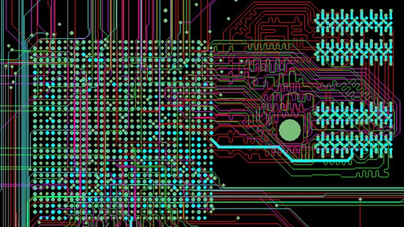
A well planned stack-up is the foundation of every successful high speed board. An 18 layer design fits enterprise servers and industrial communication equipment, 24 layers suits base stations and optical network devices, and 32 layers supports AI computing platforms, HPC servers and ultra high speed switches.
A good stack-up guarantees impedance continuity, lowers crosstalk, improves EMI performance and raises fabrication yield. Signal layers sit close to continuous ground reference planes, power planes are paired to keep return current short, and the whole structure is kept symmetrical so lamination stress does not warp the panel.
Manufacturing Technology for High Speed Backplanes
Building a high speed backplane requires precision process control. Back drilling removes via stubs that reflect high speed energy, and it is nearly mandatory for 112G and higher links. Sequential lamination supports blind and buried via structures, and mixed dielectric lamination combines low loss materials in signal zones with more economical material elsewhere when the budget demands it.
Impedance is controlled to plus or minus 5 percent on most projects and can reach plus or minus 3 percent on critical channels. Quality is verified with AOI, X-ray, flying probe, E-test, impedance coupon validation, cross sectioning, solderability tests and final inspection following IPC-A-600 and IPC-6012, using the same rigor gopcb applies to its PCBA testing services. Commercial communication equipment normally uses IPC Class 2, while aerospace, defense, medical and critical infrastructure projects specify IPC Class 3.
DFM Advice for a First Pass Success
Choose the material for the actual data rate instead of chasing low cost alone, and back drill every high speed via to remove stubs. Keep the stack-up symmetrical, balance copper distribution, and reserve enough mechanical tolerance for press-fit and high speed connectors. Differential pairs should stay over a continuous reference plane without crossing splits.
Document impedance requirements, material grades, stack-up and special process notes completely in the Gerber package. Run SI, PI and thermal simulation before release, and perform a DFM review with the manufacturer early. These steps reduce engineering change orders and dramatically improve first pass success on a board that is expensive to rework.
High Speed Backplane PCB Cost Reference
Actual pricing depends on layer count, material, size, copper weight, impedance control, back drilling, finish and testing. Prototype boards for development verification typically cost 500 to 1500 USD each. Small batches of 10 to 100 boards run about 250 to 800 USD each, and volume production above 500 boards falls to roughly 80 to 300 USD each.
Higher procurement volume, better panel utilization and standardized design continue to reduce unit cost, while premium low loss materials, back drilling and IPC Class 3 requirements push it upward. A complete PCB design and layout package with the right material plan protects both schedule and budget.
FAQ
How is a high speed backplane different from a normal multilayer PCB? A high speed backplane interconnects many function cards, with larger size, more layers, stricter impedance control and much higher data rates than ordinary boards.
Which materials should 112G and 224G systems use? Panasonic Megtron 6 and 7, Isola Tachyon, Rogers high speed laminates and Nelco SI series are recommended low loss choices.
Why does a high speed PCB need back drilling? Back drilling removes via stubs that cause reflection and insertion loss, making it essential for 112G and above.
Which IPC class do backplanes use? Commercial communication equipment usually uses IPC Class 2, while aerospace, defense, medical and critical projects use Class 3.
How long does high speed backplane production take? Prototypes need about 7 to 10 working days, small batches 10 to 15 working days, and volume production three to five weeks depending on complexity.
Get a High Speed Backplane PCB Quote
AI servers, data center switches, communication equipment, cloud platforms and HPC systems all depend on high speed backplane PCBs, and success comes from the combination of stack-up design, low loss materials, back drilling, impedance control and strict quality control. gopcb manufactures boards up to 40-plus layers and 1200 by 600 mm with impedance control to plus or minus 5 percent, laser microvias, sequential lamination, back drilling and mixed dielectric processing on Megtron, Rogers, Isola, Nelco and Shengyi materials. Send your files for a free DFM review and a high speed backplane PCB quotation.