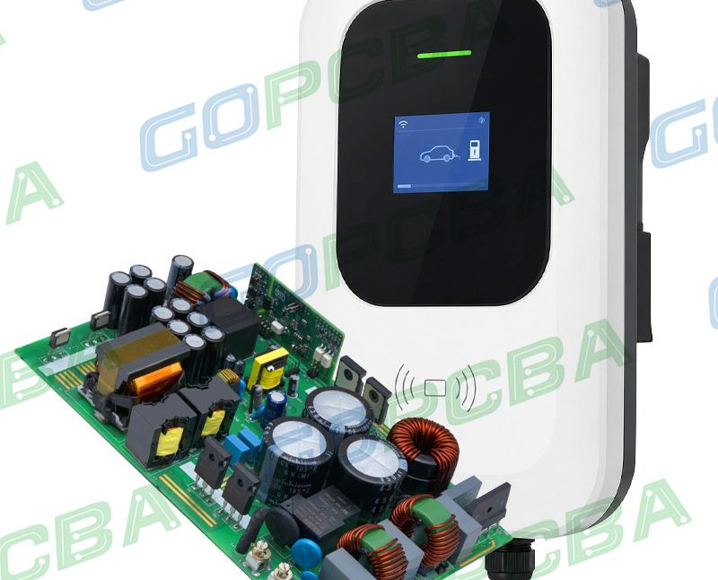
4 Layer EV Charger PCB: Design, Materials and Manufacturing Guide
Why Charging Station Control Boards Need Four Layers
Electric vehicle charging stations place tough demands on their control electronics. The board must integrate a microcontroller, communication interfaces, voltage and current sensing, relay and contactor drivers, temperature monitoring, fault protection and human machine interaction, while operating reliably outdoors for years. A two layer board can handle simple circuits, but once CAN, RS-485, Ethernet, Wi-Fi or cellular communication, RFID, displays and protection circuits share one control board, the 4 layer EV charger PCB becomes the practical solution.
This guide explains the stack-up, materials, layout, thermal management, EMC, manufacturing process, reliability and cost of 4 layer EV charger PCBs so OEMs, engineers and buyers can specify the right board for AC and DC charging equipment.
gopcb manufactures charging station boards through its PCB manufacturing service.
What Is a 4 Layer EV Charger PCB?
A 4 layer EV charger PCB is a multilayer board built from four copper layers and insulating core and prepreg materials. A typical charging station control board uses L1 as the top signal and component layer, L2 as a continuous ground plane, L3 for power distribution plus auxiliary signals and L4 as the bottom signal and component layer.
This structure provides more routing capacity in a limited area and improves return paths and power delivery for high speed signals. On a charging control board, four layers are especially useful because the design combines low voltage digital electronics with high voltage sensing, relay drive and communication in one compact system.
The stack-up can be customized for working voltage, architecture, board size, copper weight, communication rate, thermal environment and EMC requirements, which is why the layer plan should be agreed with the manufacturer during DFM rather than copied from another project.
Why Four Layers Instead of Two
Not every charger needs four layers. Simple, low component count control systems can still use double sided boards economically. When the system grows, the 4 layer EV charger PCB wins in five ways.
More routing space. Modern smart chargers combine MCU control, power management, current and voltage sampling, temperature detection, CAN, RS-485, Ethernet, Wi-Fi, 4G or 5G, RFID, display interfaces, relay and contactor drivers, and surge and ESD protection. Four layers move power, ground and signals onto different planes so the routing bottleneck disappears.
Continuous ground plane. A complete internal ground layer provides a stable, low impedance return path and shrinks signal loop area, which matters when power switches, relays and motors nearby inject noise.
Better EMC performance. Charging stations mix high voltage, high current and digital communication. Four layer construction reduces loop area, radiation, crosstalk, ground bounce, high frequency return impedance and supply noise. The layer count alone does not guarantee EMC, but it gives the designer the ground and isolation structure that makes EMC achievable.
Stronger power integrity. A dedicated power zone on layer three distributes the multiple voltage rails with lower impedance and less droop than long double sided traces, protecting MCUs, communication chips and sensors from supply noise.
Higher integration. More layers mean more components and denser layout without sacrificing signal quality, which reduces overall product size for wall boxes and DC pile housings.
Materials for Charging Station Boards
FR-4 is the most common substrate for EV charger control boards. For hot, long life or high reliability applications, high Tg FR-4 resists thermal cycling better and holds dimensional stability through repeated heating. Boards that carry charging current may use heavier copper in power zones, and metal core or thick copper constructions are available for the high current power stage where the control board is integrated with the charger module.
Surface finish selection follows the component and process needs. ENIG suits fine pitch devices and demanding solderability and is a good choice for charger boards, while HASL covers economical designs. The final choice should balance cost, SMT process, component type and product life rather than copying a default.
Design Rules for Charger Control PCBs
Safety isolation dominates the layout of an EV charger PCB. High voltage and low voltage zones must respect clearance and creepage distances, and optocouplers or isolated DC-DC converters separate the primary and secondary sides. The ground plane is split and rejoined at the isolation boundary, never run across it.
Current sensing paths should be short and use Kelvin connections so the MCU measures true drop, relay and contactor drivers need snubbers and freewheeling diodes, and the communication section, whether CAN, RS-485 or Ethernet, gets differential routing with controlled impedance. Thermistors mount close to the switching and charging components they monitor, and surge protection devices sit at the connector edge with the shortest possible path to ground.
EMC and Thermal Management
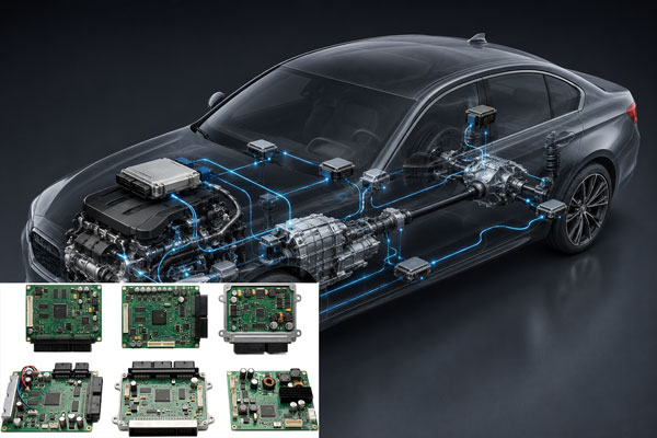
EMC for a charging station starts with the stack-up and component layout rather than shielding added at the end. A solid ground plane under the MCU and communication section, filtered power entry, isolated high voltage sensing and careful return path design keep conducted and radiated emissions within standard limits. Interface protection with TVS diodes and common mode chokes on communication lines completes the design.
Thermal management focuses on the power components and relay drivers. Wide copper pours, thermal vias and adequate spacing around high current paths lower temperature rise, and the control board should be laid out so hot power components do not heat sensitive MCU and sensor areas. For continuous outdoor operation, both the component thermal budget and the enclosure ventilation must be considered together.
Manufacturing and Quality Control
Production follows the standard multilayer flow: inner layer imaging, lamination, drilling, plating, outer layer imaging, solder mask, surface finish, electrical test and final inspection. Charging station boards are then assembled with SMT and through hole processes and verified with AOI, X-ray and functional test.
Because charging equipment is safety related, the quality system matters as much as the process. IPC Class 2 is common for commercial stations and Class 3 applies where the manufacturer specifies higher reliability. Full testing and traceability are part of gopcb’s PCBA testing service for new energy products.
4 Layer EV Charger PCB Cost Reference
Pricing depends on size, quantity, copper weight, thickness, finish, material and special processes. A typical small batch four layer FR-4 prototype runs roughly 5 to 30 USD per board, while volume pricing falls further with panel optimization. High Tg material, heavier copper, impedance control and ENIG each add a small premium that is usually worth the reliability gain on a charger that operates outdoors for a decade.
For accurate budgeting, provide Gerber files, board size, layer count, thickness, copper weight, material, finish, quantity, annual volume, impedance requirements and special reliability requirements. An early PCB design and layout review prevents expensive changes once tooling starts.
FAQ
Is a 4 layer PCB suitable for EV chargers? Yes. Four layers give more routing space, a complete ground plane, better power distribution and more flexible EMC design for mid and high complexity charging control systems.
Which material do charger boards use? FR-4 is the most common choice, with high Tg FR-4 for high temperature, long life or high reliability applications.
How much does a 4 layer charger PCB cost? Small batch four layer FR-4 prototypes are typically about 5 to 30 USD per board, with real pricing set by size, quantity, copper, finish and special processes.
Is a 4 layer board always better than 2 layers? No. Simple circuits stay economical on double sided boards, but dense systems with communication, sensors, power management and protection are easier to build reliably on four layers.
Does a charger PCB need high Tg material? Not always. The decision depends on working temperature, thermal cycling, product life, reliability requirements and cost.
Can a 4 layer PCB carry high current? Yes, with the right copper weight, trace width, allowed temperature rise and thermal design, and thick copper is available for very high current zones.
Get a 4 Layer EV Charger PCB Quote
The 4 layer EV charger PCB is the practical backbone of modern smart charging systems, combining routing density, solid grounding, power integrity and EMC headroom in one board. Real reliability comes from systematic design of materials, stack-up, creepage, thermal paths, grounding and isolation with the manufacturer from the start. gopcb provides customized multilayer PCB manufacturing for EV charging and industrial control customers, including four layer prototyping, volume production, high Tg, thick copper, impedance control and multiple finish options. Send your files for a free DFM review and a 4 layer EV charger PCB quotation today.