PCB Manufacturing Tolerances: What the Fabricator Can Hold
What a Tolerance Means on a Board
A tolerance is the range of variation that a process can hold around a nominal dimension, and on a printed circuit board it applies to almost everything that matters: the finished thickness, the width of a trace, the diameter of a drilled hole, the thickness of the plated copper, the alignment of one layer to the next and the position of the solder mask relative to the pads. None of these is exact, and none of them needs to be. The design task is to know the band each parameter will occupy and to confirm that the circuit still works at both ends of it. A design that only works at nominal values is not a conservative design; it is an untested one.
The Tolerances That Matter Most
Finished thickness. Standard builds are normally held within plus or minus ten percent of the nominal, driven by the laminate cores, the prepreg and the resin flow during lamination. Thin boards are harder to control than thick ones because the absolute variation does not shrink with the nominal value.
Trace width and spacing. The finished width depends on the artwork, the copper thickness and the etch process. An etch factor is applied to compensate, and a typical production window is around plus or minus twenty percent of nominal width, with tighter control available on impedance critical layers. Spacing matters just as much, because the minimum gap is what sets the voltage rating and the yield.
Hole size. A drilled hole is plated afterwards, so the finished diameter is smaller than the drill. Standard production typically holds the finished hole within about plus or minus 0.075 mm, and high precision and HDI work can tighten that to roughly plus or minus 0.025 mm. The tolerance has to accommodate drill wear, entry and exit material, and the plating thickness.
Copper thickness. Plated copper varies across a panel, because the current density is never perfectly uniform. A one ounce finished layer is often specified as a minimum rather than a nominal, which is the practical way to express the requirement on a power layer.
Layer to layer registration. The alignment between inner layers, and between the outer layers and the drilled holes, is one of the tightest variables in the process. It is what determines the annular ring, and therefore how much of the pad survives around the hole.
Solder mask registration. The mask opening has to be larger than the pad and centred on it, and the offset between the two is a tolerance of its own. Mask on a pad prevents soldering; a mask opening that is too large can expose an adjacent trace.
The Standards Behind the Numbers
The rigid board specifications define acceptance criteria by product class rather than by a single set of dimensions. Class 1 covers general electronics where the primary requirement is function, Class 2 covers dedicated service electronics where continued performance is expected and is where most industrial and consumer products sit, and Class 3 covers high reliability products where equipment downtime cannot be tolerated, such as aerospace, medical life support and automotive safety systems. Moving from Class 2 to Class 3 tightens the allowable annular ring, the hole wall copper, the void limits and the inspection sampling, and it changes what the fabricator has to prove rather than only what it has to build. The companion inspection standard then describes how the finished board is judged against those criteria. A drawing that names the class, the impedance targets and the critical dimensions gives the fabricator something to work with; a purchase order that only says the class leaves the electrical requirements undefined.
What Drives the Variation
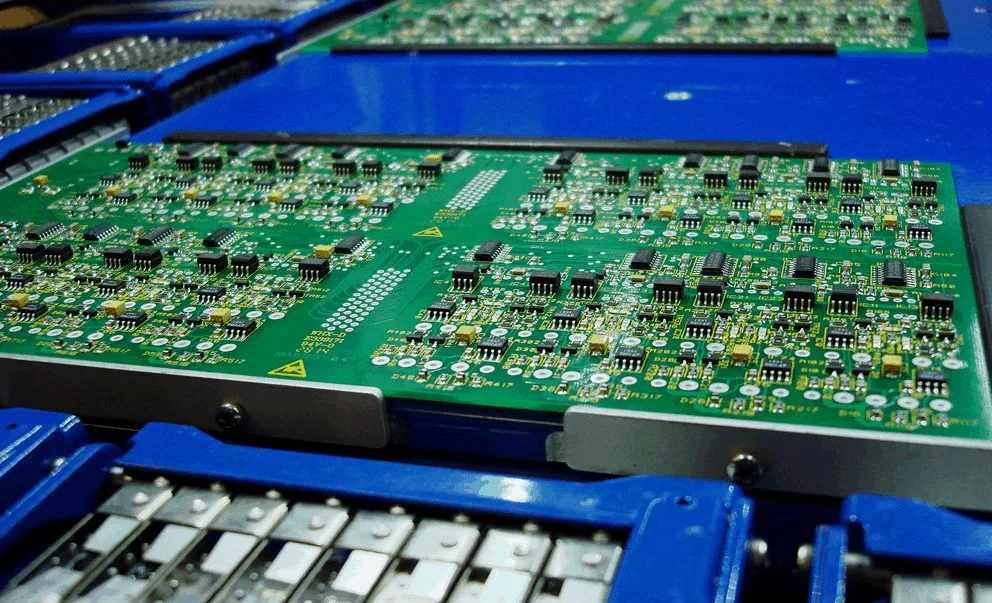
Every tolerance has a physical cause. Etch rate varies with copper thickness, panel position and bath chemistry, which is why artwork is compensated rather than drawn at nominal width. Imaging and exposure introduce their own registration error, which adds to the lamination movement of the inner layers when the panel is pressed. Drilling contributes position error from the machine, deflection of the drill and wear of the bit, and the entry and exit material affects hole quality. Plating distributes copper unevenly unless the current is balanced and the panels are adequately spaced in the bath. Lamination controls the dielectric thickness and the resin flow, and it is the step that decides whether the finished board lands inside the thickness band. Understanding which step dominates is what allows a fabricator to tighten one dimension without destabilising another.
What Tightening Costs
Tolerance is one of the few requirements that costs money in proportion to how far it is pushed. Holding a standard window is routine and included in the price. Tightening the impedance tolerance, reducing the minimum line width and gap, specifying a thicker copper layer or demanding a tighter registration requires tighter process control, more inspection and often a lower panel utilisation, because parts that fall outside the band are scrapped. The quotation reflects that in the yield. In prototype quantities the price difference between a standard and a tight build is often modest; in volume it becomes significant, which is why the requirement should be set by the circuit rather than by habit. A useful discipline is to ask, for each tightened tolerance, what happens at the far end of the band, and to relax it if the answer is nothing.
Where Tight Tolerances Are Genuinely Needed
High speed and high frequency designs need tight trace width, dielectric thickness and registration, because those three variables set the characteristic impedance and a change in any of them shows up as reflection and jitter. Automotive safety systems work to Class 3 because a failure is not recoverable, and they add their own requirements for thermal cycling and for void limits in the hole. Medical devices need tight hole tolerance and clean plating for fine pitch packages and for the reliability expectations of the application. HDI boards with microvias need tight registration because the via lands are small and the dielectric layers are thin. Power electronics need controlled copper thickness, since the current rating depends on it. In each case there is a physical reason for the requirement, which is the test that should be applied to any tolerance that is not standard.
Where Tight Tolerances Are Hard to Hold
Registration is the hardest of the group, because it accumulates error from artwork, exposure, etching and lamination, and it is bounded by the stability of the laminate itself. Hole position follows, since drilling has to land inside a pad whose size is itself a tolerance. Thin dielectrics are difficult because a small absolute variation is a large proportional change, which is why thin HDI cores are made on dedicated lines. Fine line etching is difficult because the same etch that clears a wide area nibbles at a narrow trace, so the process window narrows as the feature size falls. The practical consequence is that the tightest achievable combination of line width, spacing, registration and copper thickness is a property of the specific shop, and it should be requested as a capability rather than assumed.

How to Specify Tolerances in a Drawing
Name the applicable product class and the end product application. Give the stackup with the dielectric thickness and the tolerance for each layer, and state the impedance targets with their own tolerance and the coupon location. Specify the minimum annular ring and the hole tolerance, and say whether the hole figure is before or after plating. Specify copper thickness as a minimum where current matters. Give the mask registration requirement relative to the pad, and the surface finish thickness range. Require a certificate of conformance with the measurement data, and define what happens when a measurement falls outside the band. Written that way, the drawing becomes the quality agreement, and a dispute about whether a board conforms is settled by data rather than by argument.
FAQ
What is the standard PCB drilling tolerance? Typical production work holds the finished hole within about plus or minus 0.075 mm, and high precision and HDI processes can reach roughly plus or minus 0.025 mm.
How tight can trace width be held? Around plus or minus twenty percent of nominal is a normal production window, with tighter control offered on impedance critical layers where the artwork is compensated for the etch process.
What is the difference between Class 2 and Class 3? Class 3 tightens the annular ring, the hole wall copper, the void limits and the inspection requirements for products where downtime cannot be tolerated, and it costs more to build and to qualify.
Why does tolerance affect price? Tighter windows reduce yield and require more inspection and tighter process control, so the extra cost appears as scrap and added operations rather than as a different material.
Can I specify zero tolerance? No process can hold an exact dimension. Specify the range the circuit can tolerate, and let the fabricator work to the widest window that satisfies it.
Conclusion
Tolerances are the language in which a design tells a fabricator how much variation the circuit can absorb. Know which parameters actually drive the electrical and mechanical behaviour, express those with realistic windows taken from the process capability rather than from habit, and require measurement data so that conformance is a fact rather than an opinion. The dimensional limits that a supplier can hold are listed in PCB capabilities, the process steps that create the variation are described in PCB manufacturing, and the layout decisions that set the minimum feature sizes are covered in PCB design and layout. Confirming the stackup on a prototype PCB assembly build before volume remains the cheapest way to find out whether the tolerance stack works in 2026.