PCB Manufacturing Yield: How to Reduce Defects and Raise Output
What Yield Actually Measures
Yield is usually quoted as a single percentage, but the useful figure is first pass yield: the proportion of panels or boards that pass every inspection and test stage the first time, without rework or repair. A plant can report a high final yield while its first pass yield is low, because the difference is recovered by rework, and rework consumes capacity, adds handling and produces boards whose long term reliability is worse than boards that never needed it. The number that matters commercially is the combination of first pass yield at each stage, the cost of the rework that follows, and the scrap that cannot be recovered. Measuring only the final figure hides where the loss is occurring.
The Defects That Cost the Most
Some defects are expensive because they are frequent, others because they are only discovered late. Opens and shorts on inner layers are the classic early defect, detected at inner layer AOI before the panel is laminated, which is the cheapest possible moment to find them. Registration errors accumulate through the process and may only fail at electrical test, by which time every operation has been spent. Etch variation that pushes a controlled impedance trace outside tolerance is invisible to a visual inspection and shows up only in the coupon data. Plating voids in a hole may pass continuity test and fail in thermal cycling months later, which makes them the most expensive of all. Solder mask slivers and skips cause assembly failures at the customer rather than at the board shop. Drilling defects such as burrs, nailheads and cracked barrels sit between the two. A yield programme should rank defects by total cost rather than by count, and attack the top of that list.
Process Control Rather Than Inspection
Inspection finds defects; process control prevents them. The parameters that most strongly influence yield are the ones that drift. Etch bath chemistry and replenishment control the finished line width. The lamination press profile controls dielectric thickness, resin flow and registration. Drilling parameters and bit life control hole quality and position. Plating current density and bath additives control the distribution of copper through the barrel and across the panel. Exposure energy and artwork condition control the pattern. Each of these should have a target, a control limit and a recorded trend, because a process that is drifting produces a yield loss that appears suddenly and is then blamed on the material. Statistical process control on the coupon measurements, run after run, is the cheapest early warning available.
Design Margins and Their Effect on Yield
Yield is also a design outcome. A design that uses a 0.1 mm line width on a process whose comfortable limit is 0.15 mm will lose yield on every panel, and the loss is invisible to the designer because the boards that pass look perfect. The same applies to the minimum annular ring, the hole size relative to the drill, the spacing relative to the etch capability, and the mask dam width relative to mask registration. Working at two thirds of the supplier stated minimum is a reasonable rule for production, and the stated minimum should be treated as a prototype capability rather than a production target. Designs that respect the process limits cost slightly more board area and lose far less yield, which usually makes them cheaper overall.
Panelisation and Utilisation
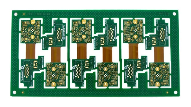
Panel design affects yield directly. Boards placed close to the panel edge are more exposed to plating non uniformity and to handling damage. Uneven copper distribution causes thickness variation across the panel and increases warpage. Insufficient material between boards makes routing and depanelisation risky, and a poor tab design produces boards that are damaged at separation rather than at fabrication. A well designed panel keeps the copper balanced, gives the router room, keeps the board borders generous and, where the design allows, uses a test coupon that belongs to the panel rather than to one board.
Finding the Loss
Yield improvement starts with data rather than with effort. Every rejection should be recorded with the stage, the defect code and the panel position, because a defect that always occurs in the same corner of the panel has a process cause, while a defect that is distributed across the panel has a materials or design cause. Recording first pass yield rather than final yield makes the rework visible, and recording the rework cost makes the priority obvious. Reviewing the three highest cost defect codes weekly, with a corrective action owner and a date, is a simple discipline that produces measurable improvement within a few months in most shops, and it costs far less than buying another inspection machine.

FAQ
What is a good first pass yield for PCB manufacturing? It depends on complexity. Simple two layer work should be in the high nineties, while dense multilayer and HDI builds naturally start lower and improve as the process matures. The trend matters more than the absolute number.
Why is reworked product a concern? Rework adds handling and thermal cycles, consumes capacity and produces boards whose reliability is worse than boards that passed first time, even when the measurement results look identical.
Can yield be improved by tightening inspection? Inspection sorts defects rather than preventing them. The improvement comes from process control and from design margins that respect the process capability.
How does design affect yield? Designs that work at the supplier stated minimum feature sizes and mask dam widths lose yield on every panel. Designing to two thirds of the stated minimum is a practical production rule.
What should be tracked first? First pass yield by stage and defect code, with the rework cost attached. That identifies where the loss occurs and which defect is worth attacking first.
Conclusion
Yield is a process outcome and a design outcome at the same time, and it is best managed by measuring first pass yield by stage, ranking defects by cost, and controlling the parameters that drift. Keep the design inside the production capability rather than at the prototype limit, balance the panel so that plating and lamination behave, and review the data weekly with an owner for each corrective action. The production limits that a design should leave margin against are listed in PCB capabilities, the layout decisions that set those margins belong in PCB design and layout, and the control points that determine the result are described in PCB manufacturing, with the management system behind them in quality management. A prototype PCB assembly build tests the design margins before they are locked into a production lot in 2026.