Back Drilling PCB: Why Via Stubs Matter at High Speed
The Stub Is the Problem
A plated through hole that connects the outer layers of a thick board also passes through every layer in between. If the signal only needs to travel between two of those layers, the unused portion of the barrel below the connection is a resonant piece of copper hanging off the signal path, and at high frequency it behaves as an open ended transmission line stub. The stub reflects energy back into the channel, creating a notch in the insertion loss at the frequency where the stub is a quarter wavelength, and it adds jitter that grows with the data rate. At a few hundred megabits per second the effect is negligible. At ten gigabits per second and above in a thick backplane it can close the eye entirely, and no amount of equalisation at the receiver fully recovers the lost margin.
How Back Drilling Works
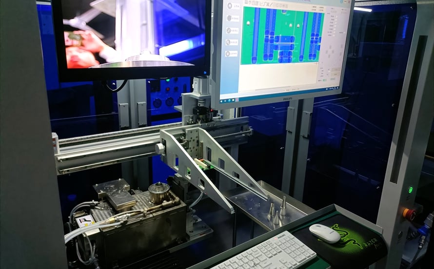
Back drilling removes the unused portion of the barrel after plating. A drill of slightly larger diameter than the via is run from the opposite side of the board to a controlled depth, cutting away the stub and leaving the barrel intact through the layers that actually carry the signal. The depth is set so that the remaining stub is short enough to push the resonance well above the frequency band of interest, typically to a residual length of a few tenths of a millimetre. Because the process removes copper that is not needed for connection, the electrical result is a via that behaves almost like a blind via, at a fraction of the cost of building the stack with sequential lamination.
Depth Control and Tolerance
The process is a controlled depth drilling operation, and the tolerances are what make it difficult. The board thickness varies across the panel, the dielectric layers vary with the press, and the drill has to stop at the right depth in every hole. The specification is usually written as a maximum remaining stub length plus the clearance to the last connected layer, and the fabricator has to hold both. A drill that goes too deep damages the connection it was supposed to preserve; a drill that does not go deep enough leaves a stub that may or may not matter at the target data rate. The anti pad and the pad geometry around the via have to allow for the larger drilling diameter, which is one of the reasons back drilling is designed into the stackup rather than added afterwards.
Design Rules and Stackup Consequences
Back drilling only makes sense on through vias that terminate well above the bottom of the board. If the signal runs to an inner layer near the far side, the stub is already short and there is nothing to remove. In practice it is applied to backplane and midplane designs where signals enter on the top layer and terminate in the middle, and it is normally applied to all signal vias in the channel rather than selectively, because an unback-drilled via in the same channel will dominate the loss. The via pad and the anti pad must be sized for the back drill diameter, and the routing near the via must keep clear of the larger hole. Where layer pairs are used, the fabricator may need to know which side is drilled so that the tool can approach from the correct face.
Manufacturing Effects and Inspection
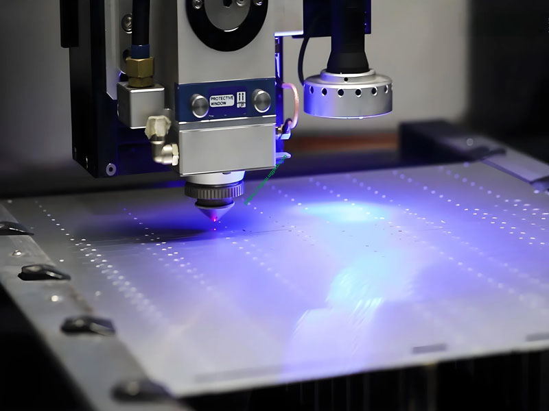
Back drilling is an extra operation with its own equipment and its own consumable drills, and it happens after plating and before or after outer layer processing depending on the process flow. It leaves a countersink on the surface, which must be considered when the via sits under a component or near a fine pitch device, and it changes the surface topography that the solder mask has to cover. Inspection is done by cross section on a coupon or a sample, measuring the remaining stub and confirming that the drill did not approach the connected layer too closely. Because the measurement is destructive, the process control relies on depth setting, drill wear monitoring and periodic cross sections rather than on inspecting every board.
Cost and When It Is Worth It
Back drilling adds cost in several ways: an extra operation and setup, a dedicated drill program, tighter depth control, a yield impact from occasional over drilling, and the need to verify the result by cross section. The premium is often quoted per via or as a percentage uplift on the board, and it becomes significant on a board with thousands of vias. It is justified when the channel budget cannot be met any other way: a thick backplane at high data rate, a long trace that cannot be shortened, or a link whose margin is already thin. On a thin board, or where the via already terminates close to the bottom layer, the same money is better spent on the stackup, the laminate or the connector. The honest test is to simulate the channel with and without the stub and see whether the eye opens enough to matter.

FAQ
What is a via stub? The unused portion of a plated through hole barrel below the layer where the signal terminates. It acts as a resonant transmission line stub at high frequency.
How deep should back drilling go? Deep enough to leave a residual stub short enough that its resonance is above the band of interest, typically a few tenths of a millimetre, while keeping a safe clearance to the last connected layer.
Does back drilling damage the connection? Not if the depth is controlled. Over drilling is the main yield risk, which is why the process is verified by cross section rather than by appearance.
Is back drilling needed on every board? No. It matters when a through via has a long stub relative to the data rate. On thin boards or vias that terminate near the far side, the benefit is small.
What does back drilling cost? An extra drilling operation with a dedicated program and depth control, a yield impact, and cross section verification. It is usually quoted per via or as a percentage uplift.
Conclusion
Back drilling removes the copper that is not needed for connection and is the cheapest way to make a through via behave like a blind via on a thick board. Specify the maximum remaining stub and the clearance to the connected layer, size the pads for the larger drill, and confirm the result by cross section rather than by confidence. The drilling capability and the achievable stub tolerance are part of PCB capabilities, the stackup and via planning belongs in PCB design and layout, and the process sequence is described in PCB manufacturing. A prototype PCB assembly build with measured channel data confirms whether the stub removal bought the margin the simulation predicted in 2026.