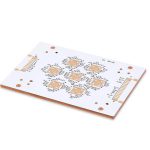
Surge and ESD Protection Layout
Two Different Threats
Electrostatic discharge and surge are different events with different energies and different timescales, and a protection design has to account for both. An electrostatic discharge is a short, fast event with a rise time measured in hundreds of picoseconds and a current that can reach tens of amps; the damage it does is usually to a semiconductor junction that sees the voltage before the protection responds. A surge, such as a lightning-induced transient on a cable, is slower and carries far more energy, and the damage is often thermal. A device that is good at one is not necessarily good at the other, which is why a design often uses two devices with different characteristics in a coordinated arrangement.
The Protection Device
The usual devices are a transient voltage suppressor, a metal oxide varistor, a gas discharge tube and a steering diode network. A TVS diode responds quickly and clamps the voltage at a defined level, which makes it the standard choice for signal lines and for the first line of defence against electrostatic discharge. A varistor has a higher energy capability but a slower and softer clamp. A gas tube can handle a large surge but is far too slow to protect against an electrostatic event on its own. The device parameters that matter are the standoff voltage, which has to be above the normal operating voltage with margin, the breakdown voltage, the clamping voltage at the expected surge current, the capacitance, which must not disturb the signal, and the response time.
Placement and the Discharge Path
The protection device has to be between the threat and the circuit, which in practice means immediately at the connector, before any other component. Placing it after a series element such as a resistor or a ferrite bead is a common error: the series element slows the edge and adds impedance, so the protected circuit sees a higher voltage than the device was designed to clamp, and the protection may never conduct at all. The discharge path matters as much as the placement. The current from the transient has to flow from the connector, through the device, into the reference, and back to the source of the transient, and the impedance of that path determines how much voltage appears across the circuit. A short, wide, direct path to a solid ground plane is what makes the protection work.
Trace Length and Inductance
A transient is a fast event, so the impedance of the connections is dominated by inductance rather than resistance. An extra few millimetres of trace between the connector and the protection device adds nanohenries, and at the rate of rise of an electrostatic discharge that inductance develops a significant voltage, which appears across the protected circuit. This is the reason a protection device placed a centimetre inside the board can be less effective than one placed at the pin, and the reason the ground connection should be made with a via directly at the device rather than by a trace running to a distant via. The rule is to treat the connection to the protection device as part of the protection itself, and to keep it as short as the layout allows.
Grounding
The reference that the transient is discharged into has to be able to accept it without moving. That means a solid plane, a low impedance connection and, where the product has a chassis, a deliberate bond between the board reference and the chassis at the connector. Where the board reference floats relative to the chassis, the transient current has to find another path, and the path it finds is usually through the circuit. The bond is often made with a capacitor or a resistor in parallel, which passes the high frequency transient while keeping the direct current isolation, and its position relative to the connector is what determines whether the transient is diverted before it reaches the circuit.
Protecting a Connector
A connector with many pins needs a protection strategy per pin rather than a single device, since the transient can arrive on any of them. The practical arrangements are an array device that protects several lines in one package, a row of discrete devices placed immediately behind the connector on a ground plane, and an integrated connector with protection built in. Where the signals are differential or high speed, the capacitance of the protection becomes a design constraint, and a device with a low capacitance is used even at the cost of a lower energy rating, with a second stage behind it for the slower surge. Where the connector carries power, the protection has to handle the continuous current as well, and the device is chosen for that rating first.
Measuring the Result
Protection is verified by applying the specified test waveform to the connector and confirming that the circuit survives, which means the test is done at the system level with the product in its normal configuration. The useful diagnostic when a design fails is to look at the path the current took, since a failure usually means the current bypassed the protection rather than that the device was inadequate. Where a design passes the test but is marginal, the improvement that usually works is shortening the connections and improving the ground rather than fitting a larger device.
Protection and the Assembly Sequence
The protection devices are usually placed in the same reflow pass as the rest of the components, which means they must survive the reflow temperature and, more importantly, must not be damaged by the assembly process itself. Many protection devices are sensitive to electrostatic discharge during handling and placement, and a device that is damaged during assembly may pass the functional test and fail later in the field, which makes the assembly handling part of the protection strategy. The practical measures are to specify devices with a defined handling requirement, to use grounded equipment, and to test the protection function at the end of the line rather than only the circuit function. Where a design has protection that cannot be verified in production, the escape risk is carried into the field, and it is worth considering whether the test can be added.
FAQ
Why does protection sometimes not work? Because the transient finds a path around the device, usually through a long ground return or a series element placed before it.
Where should the device be placed? Immediately at the connector, between the threat and everything else, with the shortest possible connection to the reference.
Does a bigger device protect better? Not necessarily. The limiting factor is usually the impedance of the connections rather than the device rating.
What is the difference between ESD and surge? ESD is a very fast, low energy event; a surge is slower and carries far more energy. Different devices suit each.
Why bond the reference to the chassis? So that the transient current has a defined path that does not run through the circuit.
Conclusion
Protection works when the transient is forced through the device on a short, low impedance path, so the placement, the return path and the reference bond matter more than the device rating. Put the device at the connector, keep the ground connection short, coordinate devices for the two threat types and verify at the system level. Protection layout is part of PCB design and layout, the assembly belongs to SMT PCB assembly, and the verification is part of PCBA testing. Compliance testing is normally planned alongside prototype PCB assembly in 2026.