Test Coupons and Impedance Verification
What a Coupon Is For
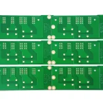
A test coupon is a structure on the production panel that has no function in the product, and that exists to be measured. It carries the same traces, the same stackup and the same process as the product, so that a measurement on the coupon describes what the product received without destroying a product board. For a controlled impedance design the coupon is the evidence that the requirement was met, and for a plating requirement it is the section that shows the barrel’s thickness. The coupon is therefore a quality tool rather than a piece of waste area.
Designing the Coupon
The coupon should represent the product’s critical features. For impedance it should carry the same trace width and spacing, the same layer and the same reference plane arrangement as the product’s controlled lines, and it should be long enough for the measurement method to be valid. For plated holes it should carry the smallest diameter and the greatest aspect ratio, because those are the hardest to plate. The coupon should be placed on the panel where the process conditions are representative, and it should be marked so that it can be traced to the lot. A coupon that is convenient rather than representative produces a comfortable result that means little.
Measuring Impedance
Impedance is measured by time domain reflectometry, in which a fast edge is launched into the line and the reflection is analysed, or by a frequency domain method such as a network analyser. Both require a coupon whose geometry is known and a launch that does not add its own impedance. The measurement should be made on the line rather than at the connector, and the result should be compared with the specification and with the design’s prediction. The measurement’s uncertainty comes from the launch, the coupon’s geometry and the instrument’s calibration, so the method should be defined and repeated consistently.

What the Coupon Proves
A coupon measurement proves that the process produced the intended geometry and material on that panel. It does not prove that every trace on the product is within tolerance, since the etching, the plating and the lamination vary across the panel, but it does establish that the process is under control. Where several coupons are placed at different positions on the panel, the variation across the panel becomes visible, which is useful for a large panel or a critical design. The results should be recorded with the panel’s identity and compared across lots, since a trend is more informative than any single measurement.
Coupons for Plating and Microsection
The same coupon or a second one is used for the microsection. It carries the plated holes and it is sectioned after the plating, so that the barrel’s thickness and the laminate’s condition can be measured. The coupon should include the smallest hole and the highest aspect ratio, since a larger hole will always plate better and will not reveal the process’s limit. The section should be taken from the coupon rather than from a product board wherever possible, because the product board is the deliverable and the coupon is the sample.
Coupons for Solderability and Cleanliness
A coupon can also be used for the solderability test of the surface finish and for the cleanliness measurement. For solderability, a coupon with the same finish as the product is tested by a wetting balance or by a dip and inspect method, which shows whether the finish is active. For cleanliness, a coupon that has been through the same assembly process can be rinsed and the extract measured, which avoids immersing a product board. Both uses require the coupon to be processed exactly as the product is, which is the point of having it.
Managing and Recording
The coupon’s results belong with the lot’s records. The design of the coupon, the measurement method, the instrument and its calibration, and the measured values should be recorded so that a later comparison is meaningful. Where the customer requires a certificate, the coupon data is usually the evidence that accompanies it. Where a coupon fails, the lot’s disposition should be decided from the data rather than from the coupon alone, since the coupon is a surrogate for the product and its failure indicates a process problem rather than a specific board’s defect.
Coupons for Microvia and HDI Structures
Where the design uses microvias or a sequential build, the coupon has to represent those structures too, because their plating and their registration are different from a through hole. A coupon with a microvia should carry the smallest via and the stack that the product uses, and it should be sectioned at the same stage as the product so that the intermediate steps are visible. The failure modes differ as well: a microvia can separate at the interface with the target pad, and a stacked microvia can crack between the layers. The coupon is often the only place where those structures can be examined without destroying a product board, which makes its design part of the HDI programme rather than an afterthought.
FAQ
What is a test coupon for? To measure the process’s result on the panel without destroying a product board.
What should an impedance coupon carry? The same trace geometry, layer and reference plane arrangement as the product’s controlled impedance lines.
How is impedance measured? By time domain reflectometry or a frequency domain method, with a defined launch and calibration.
Does a coupon prove every trace is in tolerance? No, it proves the process is under control; placing coupons at several positions shows the variation.
Why put the smallest hole on the coupon? Because it is the hardest to plate and reveals the process’s limit, which a larger hole would hide.
Conclusion
A test coupon is the sample that represents the product, so design it to carry the critical features and record what it measures. Compare the results across lots. Coupon design belongs to PCB manufacturing, the impedance requirement comes from PCB design and layout, and the acceptance is defined under quality management. Coupons for a new product are specified during prototype PCB assembly in 2026.