Depaneling Methods and Their Defects
Why Depaneling Matters
The panel has to be separated into boards after assembly, and the separation applies a mechanical stress to the assembly. That stress can crack a solder joint, chip a component, crack a laminate or delaminate a layer, and the damage may not appear until later. Depaneling is therefore a process with its own defects, and the method and the panelisation design together determine how much stress the boards see. A separation method chosen for speed, without regard to the stress, is a common source of intermittent failures that no inspection finds.
V-Scoring
V-scoring cuts a V shaped groove on both sides of the board along the separation line, and the board is snapped along the groove. It is fast and cheap, and it suits a rectangular board with a straight separation line. Its limits are the stress it imposes, since the snap bends the board along the line and the stress concentrates near the groove, and the requirement that the groove be on both sides and along straight lines. A component placed near the score line experiences the full bending stress, and a brittle component or a large one may crack. The groove’s remaining material determines the stiffness and therefore the force required, and it should be specified rather than left to the tool’s setting.
Routed Tabs
Routing cuts the board free with a milling cutter, leaving small tabs that hold the board until they are cut or broken. The routing itself applies little stress, because the cutter removes the material rather than bending it, and the tabs are placed where the stress is acceptable. The tab’s size and position are the design variables: a tab near a component transfers the separation stress to it, and a tab that is too large requires more force to break. Where the tabs are cut with a cutter, the stress is small; where they are broken by hand or with a tool, the force can be large, which is why the tabs should be placed and sized to break cleanly.
Laser and Punch Separation
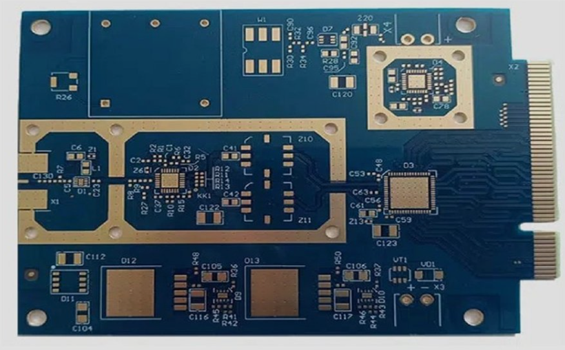
A laser cuts the board free without applying a mechanical stress, which suits a thin or a brittle board and a design with a component close to the edge. It is slower and more expensive per panel, and the cut edge may have a heat affected zone that should be considered. A punch or a shear is fast and applies a clean cut, but the force is high and the stress is concentrated along the cut, so the component placement and the panelisation have to accommodate it. A punch requires a tool for the board’s outline, which adds a cost that only a high volume justifies.
Stress and the Layout
The layout determines how much the depaneling matters. A component placed close to a score line or a tab experiences the full bending moment, and a ceramic capacitor or a glass bodied component is the most at risk. The rule is to keep the components away from the separation line by a distance that reflects the method’s stress, and to place the tabs where the board is stiff rather than where it is flexible. The board’s thickness and its material also matter: a thin board bends more for the same force, and a brittle laminate cracks sooner. The layout rules should state the clearance for each separation method.
Detection and Its Difficulty
Depaneling damage is difficult to detect. A cracked joint may still measure as continuous, a micro crack in a laminate may be invisible, and a chipped component may function. The damage appears later, after a thermal cycle or a vibration, as an intermittent fault. That is why the detection cannot be relied on and the prevention has to be built into the method and the layout. Where a product has a history of a failure that appears after assembly, the depaneling should be examined as a possible contributor, and the stress at the separation line should be measured rather than estimated.
Choosing a Method
The choice follows the board, the volume and the component placement. A simple rectangular board at volume suits V-scoring, provided the components are clear of the line. A board with an irregular outline or components near the edge suits routing or laser. A thin or brittle board suits laser. A high volume with a simple outline may justify a punch tool. The method’s cost per panel, its speed and its stress should all be considered, and the panelisation should be designed with the method in mind rather than the method chosen after the panelisation is fixed.
Handling After Separation
The separated board is a finished assembly, and the handling from that point is part of the risk. The boards should not be stacked directly, because a component or a connector can damage its neighbour, and they should not be placed where a static charge can build. Where the separation leaves a burr or a sharp edge, the edge can damage a component or a finger, and it can also indicate that the score or the tab was not correct. The boards should be inspected after separation for the damage that the process can cause, and the inspection should be part of the flow rather than an occasional audit.
FAQ
What is the difference between V-score and routing? V-scoring bends the board to snap a groove; routing cuts the board free and leaves tabs.
Which method stresses the board most? V-scoring and a punch, because they apply a bending or a shear force along the separation line.
Why keep components away from the separation line? Because the stress there is highest, and a brittle or a large component can crack.
Why is depaneling damage hard to detect? A cracked joint may still measure continuous, and the failure appears later after a thermal cycle or vibration.
When is laser separation justified? For a thin or brittle board, or a design with a component close to the edge, where the mechanical stress cannot be tolerated.
Conclusion
Depaneling is a source of stress, so choose the method for the board and place the components clear of the separation line. Prevention beats detection. Separation and handling belong to PCB assembly, the panel design is part of PCB manufacturing, and the acceptance is part of quality management. Panel and separation design for a new product is set during prototype PCB assembly in 2026.