Blind and Buried Vias in Multilayer Boards
What the Two Terms Mean
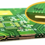
A blind via starts at an outer layer and ends at an inner layer, so it is visible from one side only. A buried via connects two inner layers and is not visible from either surface. Both exist to make a connection without passing through the whole board, which frees routing space on the layers they do not penetrate and removes the stub that a through hole would leave. A microvia is a small blind via, usually formed by laser, and it is the building block of a high density interconnect design.
How They Are Made
A blind or buried via requires a sequential lamination. A subset of the layers is laminated and drilled, the vias are plated and the copper is patterned, and then the remaining layers are laminated on top and the process repeats. Each additional lamination cycle adds a press, a drilling operation, a plating step and the registration and inspection that go with them, which is why the cost rises sharply with the number of sequential steps. A design with a single lamination cycle is the least expensive; a design with two or three costs several times as much and takes longer, and the design should justify each one.
The Design Rules
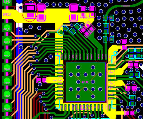
The rules follow from the process. A buried via’s layers have to be contiguous in the lamination sequence, since the connection is made before the outer layers are added. A blind via’s depth is limited by the aspect ratio the process can plate, which for a laser drilled microvia is much higher than for a mechanically drilled one. The via’s position has to respect the registration tolerance between the layer sets, which is larger than the tolerance within a set. And the via has to land on a pad with an adequate capture, since a laser drilled via that misses the target pad creates an open or a weak connection.
Microvias and Their Reliability
A microvia is small enough that its reliability depends on the target pad’s geometry and the interface between the via and the pad. The failure mode is a separation at the interface, often at the base of the via, when the laminate expands during thermal cycling. Stacked microvias, where one via sits directly on another, concentrate the strain and are the most demanding; staggered vias distribute it. The design rules that improve the reliability include a larger capture pad, a shallower via, a staggered rather than a stacked arrangement where the routing allows it, and a plating that is ductile. Where the product sees thermal cycling, the microvia’s reliability should be qualified by test rather than assumed.
Registration and Tolerance
Each lamination cycle introduces a registration tolerance between the layer sets, and the design’s via capture pads have to accommodate it. That means the pad’s annular ring for a blind or buried via is usually larger than for a through hole at the same layer count, which consumes routing space and can offset the space that the via was meant to free. The tolerance should be obtained from the fabricator rather than assumed, and the design’s pad sizes should be checked against it. Where the tolerance is tight and the pad is small, a registration error produces an open or a reduced connection that the electrical test may not find.
Stackup and Layer Assignment
The stackup is the design’s main lever. Assigning the high speed signals to layers that can be connected with a short via reduces the stub and the loss, and grouping the power and ground layers so that they can be connected with a buried via pair improves the plane’s impedance. The layer count, the lamination sequence and the via types should be planned together, and the plan should be discussed with the fabricator early, because the sequence determines the lead time and the cost as much as the layer count does. A stackup that is chosen for the electrical requirement and then found to need three lamination cycles is an expensive surprise.
Verification
The verification is by a microsection that shows the via’s shape, its capture and the interface with the target pad, and by the coupon’s design which should include the smallest via and the most demanding stack. Because the section is destructive, the coupon is the sample and the product board is not sacrificed. The reliability is verified by thermal cycling with continuous monitoring, and the failure analysis of any failure is by a section at the failure site. Where the design uses stacked microvias, the cycling test is the evidence that the stack is acceptable, since the calculation is less reliable for that geometry.
Via Fill and Tenting
A via that must be soldered over, or that sits in a pad, is usually filled and capped, and the fill’s material and its planarity determine whether the pad can be used. A filled and plated via is the most robust and the most expensive; a filled with a non conductive paste and a copper cap is common on a via in pad; a tented via is simply covered by the mask, which is adequate where nothing has to be placed over it but which traps the flux and the cleaning fluid. The choice should follow the function: a via that carries a component, a via that must be flat and a via that only needs protection are three different requirements.
FAQ
What is the difference between a blind and a buried via? A blind via reaches an outer layer; a buried via connects inner layers only.
Why do they cost more? Because each requires a sequential lamination cycle with its own drilling, plating and registration steps.
Why is a microvia’s capture pad critical? A laser drilled via that misses or barely reaches the target pad creates an open or a weak connection.
What is the risk with stacked microvias? The strain concentrates at the interface, so the reliability depends on the capture and the plating.
How should the stackup be planned? With the fabricator and with the lamination sequence in view, since the sequence drives the cost and the lead time.
Conclusion
Blind and buried vias free routing space and shorten the electrical path at the cost of a sequential lamination, so plan the stackup with the fabricator. Verify with a coupon. Via and stackup design belongs to PCB design and layout, the sequential build is described under PCB capabilities, and the acceptance is part of quality management. HDI stackups are first built during prototype PCB assembly in 2026.