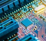
Advanced Packaging Interconnect Density Upgrade Forces PCB and IC Substrate Iteration
The boundary between advanced packaging and PCB is becoming increasingly blurred
In the past, chip packaging and circuit boards each managed their own area. Packaging substrates handled micron-level fine circuits, while PCB was responsible for board-level interconnection at the tens of micrometers level. But after the popularization of Chiplet architecture and 2.5D and 3D packaging, the situation changed. A chip package may contain multiple chiplets such as GPU and HBM. The number of I/Os has skyrocketed, and solder ball pitch has shrunk from the traditional 1.0 mm or more to 0.4 to 0.5 mm.
PCB Is Being Forced to Move Toward Semiconductors
The chip pins have become denser, and PCB must be able to catch up. Traditional line width and spacing above 75 micrometers are no longer sufficient. Taking 1.6T optical modules as an example, the minimum line width and spacing must shrink to 15 micrometers. In new packaging processes such as CoWoP, PCB even has to directly assume part of the substrate function, and line width and spacing must be controlled at 15 to 20 micrometers.
The traditional subtractive method has hit a wall on this path. It etches away unnecessary parts on thick copper foil. The finer the circuit, the more serious the side etching, and the cross-section of the resulting circuit looks like a trapezoid. To break through this barrier, modified semi-additive process, or mSAP, must be used. First, a very thin base copper is laid on the board. LDI equipment is used to precisely expose the circuit pattern. Then, electroplating is used to thicken the circuit area. Finally, the thin copper between circuits is quickly etched away. The circuit cross-section is closer to a rectangle, and wiring density and impedance consistency are improved.
The application scope of mSAP is rapidly expanding from smartphone substrate-like PCBs to AI servers, optical modules, and advanced packaging. Aeon Securities estimates that the global mSAP PCB market size will increase from about 4.5 billion US dollars in 2025 to 7.2 billion US dollars in 2028.
Substrates Are Also Moving Toward More Extreme Precision
PCB is reaching upward, and IC substrates are not idle either. For organic substrates under CoWoS packaging, line width and spacing are advancing from 10 micrometers to 8 micrometers and 5 micrometers. Kyocera’s FC-BGA substrate has already achieved 9 micrometer line width and 12 micrometer line spacing. The product precision of domestic manufacturer Qinghe Dianke has reached the 8 micrometer level. The number of IC substrate layers is also increasing. Over the past two decades, IC substrate size has increased by about 20 times, and the number of layers has increased by more than 4 times.
A thin board is becoming a key bottleneck connecting chips and systems.
Boundaries Are Disappearing, and the Supply Chain Is Being Reshuffled
The technical boundary between PCB and IC substrates is disappearing. The materials used by both are becoming more and more similar: low dielectric loss build-up films, chemical copper plating, and laser microvia technology. A new technology continuum has emerged among traditional PCB, bridge substrates, and IC substrates.
The impact of this round of upgrading on the supply chain is structural. The equipment end benefits first. Drilling equipment needs microvia processing capability of 60 to 80 micrometers, and LDI equipment requires imaging precision of plus or minus 0.5 micrometers. Barriers at the manufacturing end are also rising. The smaller the line width and spacing, the more any deviation in any process will be amplified, ultimately reflected in the gap in yield and gross margin. Major global substrate manufacturers, including Ibiden and Shinko of Japan, Unimicron of Taiwan, and Samsung Electro-Mechanics of South Korea, are all expanding mSAP production lines on a large scale.
From 75 micrometers to 15 micrometers, the difference is not just a few processes, but a complete generation change of the entire process system. Whoever can first run through this system will be able to get the largest share of the next round of AI hardware cake.
Gopcba provides professional PCB manufacturing, PCB assembly, prototype PCB assembly, low-volume PCB assembly, high-volume PCB assembly, SMT PCB assembly, through-hole PCB assembly, mixed-technology PCB assembly, flex PCB assembly, PCB design layout, components procurement, rapid PCBA prototyping, conformal coating, PCBA testing, box build assembly, wire cable harness assembly, medical PCBA, telecommunications PCBA, energy PCBA, industrial PCBA, artificial intelligence PCBA, Internet of Things PCBA, PCB capabilities, and PCBA capabilities. You can also visit our blog, learn about us, see why us, review our quality management, or contact us for more information.