Aerospace-Grade High-Reliability PCB Design: Gold Finger Plating Selection, Ionic Contamination Control, and Conformal Coating Compatibility
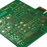
In aerospace electronic systems, printed circuit boards serve as the core carrier for high-density interconnection, high-reliability signal transmission, and extreme environment adaptability. Their design does not allow the slightest error. Spacecraft payload boards with mission cycles of more than 15 years, operating temperature ranges spanning minus 65 to plus 125 degrees Celsius, total ionizing dose of 100 krad Si, and continuous exposure to high-frequency vibration and microgravity environments place requirements far beyond industrial-grade and even military-grade standards on PCB material systems, surface treatment, cleanliness, and protective processes. Among them, the selection of gold finger plating directly affects connector insertion and extraction life and contact resistance stability. The level of ionic contamination is directly related to electrochemical migration risk under long-term bias. The interface compatibility of conformal coating with plating and solder mask determines the adhesion and pinhole rate of the protective layer during thermal vacuum cycling. The three are not isolated parameters but constitute the key coupling chain of electrical, mechanical, and chemical collaborative reliability for aerospace-grade PCB Design.

Multilayer Structure Design and Thickness Gradient Control of Gold Finger Plating
In aerospace applications, ENIG, or electroless nickel immersion gold, is strictly prohibited in gold finger areas because its phosphorus content fluctuations cause uneven amorphous nickel layer, which is prone to microcracks under thermal stress and becomes a copper diffusion channel. The mainstream solution is electrolytic hard gold plating. The typical structure is: copper substrate, 150 to 200 nm nickel barrier layer with purity of 99.99 percent or more and phosphorus content less than 0.015 percent, and 0.76 to 1.27 micrometers hard gold layer containing 0.1 to 0.3 weight percent cobalt with Vickers hardness of 180 HV or more. The nickel layer must be annealed at 200 degrees Celsius for 1 hour to eliminate electroplating internal stress and improve grain boundary density. The cobalt content of the gold layer must be strictly calibrated by ICP-MS. Too low results in insufficient wear resistance, and too high increases brittleness. Measurements show that when cobalt is greater than 0.35 weight percent, the contact resistance increment after 500 insertion and extraction cycles exceeds 30 milliohms. A certain remote sensing satellite main control board used 0.89 micrometers hard gold plus 200 nm nickel. After HALT testing from minus 65 to 125 degrees Celsius with 15 minute ramp and 20 cycles, the gold layer showed no peeling, insertion and extraction force attenuation was less than 8 percent, and contact resistance standard deviation was 2.1 milliohms or less at 48 points.
Quantitative Control of Ionic Contamination and Trace Analysis Methodology
IPC-J-STD-001G sets the upper limit of ionic contamination for aerospace-grade PCB at 0.20 micrograms per square centimeter NaCl equivalent, only one fiftieth of the commercial-grade limit of 10.06 micrograms per square centimeter. This indicator must be verified at five key nodes: bare board, after SMT reflow, after cleaning, before conformal coating, and after aging. Detection must use ion chromatography, or IC, rather than the traditional ROSE method. The latter cannot distinguish specific anions such as Cl, Br, and SO4 and is completely insensitive to organic acid radicals such as formate and acetate. In actual engineering, it has been found that the pyrolysis product of diethylene glycol monobutyl ether, or BDG, from no-clean solder paste residue can generate formate, which accelerates migration under 85 degrees Celsius and 85 percent RH, forming Cu2O dendrites. A certain deep space probe power management board once experienced intermittent bus short circuits in the third year in orbit because BDG residue was not detected by IC. Therefore, aerospace projects mandatorily require that the Cl peak area proportion in IC spectra be less than 40 percent, and the total amount of formate and acetate be 0.05 micrograms per square centimeter or less. The cleaning process must match ultrapure water with TOC less than 5 ppb and resistivity of 18.2 megohm centimeters or more, and megasonic assistance with frequency of 1.2 MHz and power density of 0.3 W per square centimeter, ensuring ion removal efficiency at the bottom of blind holes of more than 99.97 percent.

Interface Energy Matching and Thermomechanical Failure Mechanism of Conformal Coating with Plating and Solder Mask
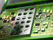
Aerospace PCB conformal coating prohibits acrylic types due to low Tg and fast UV aging, and polyurethane types due to easy hydrolysis and reaction with ENIG nickel layer to generate Ni(CO)4. The only currently certified material is modified parylene C vapor deposition coating. Its thickness control precision reaches plus or minus 0.1 micrometers, with a target of 25 plus or minus 2 micrometers. Selective masking must be implemented in gold finger areas. Coating intrusion in unmasked areas will cause excessive insertion and extraction force and poor contact. The key challenge lies in the interface bonding of parylene with FR-4 substrate, OSP copper surface, and hard gold layer of gold fingers. XPS analysis confirms that there is about 0.8 nm thick AuO2 natural oxide layer on the hard gold surface. Chlorine atoms in parylene molecular chains can form weak coordination bonds with it, achieving peel strength of 1.8 N per mm per ASTM D903. However, if the nickel barrier layer is exposed due to gold layer wear or over-etching, parylene will undergo dechlorination reaction with Ni, generating NiCl2 crystalline particles and causing local coating blistering. A certain Mars lander navigation computer board showed blisters with a diameter of 30 to 50 micrometers at the edge of gold fingers after thermal vacuum cycling at 10 to the minus 3 power Pa from minus 80 to plus 70 degrees Celsius. SEM-EDS confirmed it was a NiCl2 enriched area. The solution is to use a double-layer masking process: first plate gold and then coat the entire board, then laser open the window to expose gold fingers, and finally re-plate 0.2 micrometers soft gold with purity of 99.999 percent to cover oxidation defects.
Necessity of Multi-Physics Collaborative Verification and Test Profile Design
A single environmental test cannot expose coupling failures. Aerospace PCB must perform three-stage superimposed verification. The first stage is electrical bias accelerated testing at 85 degrees Celsius and 85 percent RH with bias voltage at 70 percent of rated voltage for 1,000 hours, monitoring leakage current and insulation resistance changes. The second stage is thermal vacuum and vibration composite testing at 10 to the minus 3 power Pa, minus 65 to plus 125 degrees Celsius, and 20 to 2,000 Hz random vibration with Grms of 12.5, focusing on gold finger fretting wear and parylene interface delamination. The third stage is electrical performance retesting after proton irradiation with 50 MeV protons and fluence of 1 times 10 to the 11th power p per square centimeter, evaluating radiation-induced dielectric polarization attenuation. A certain low earth orbit communication satellite payload board found in the second stage that at the 1,500 Hz resonance frequency point, a 0.5 mm long microcrack appeared at the interface between parylene coating and solder mask. FIB-TEM analysis showed that the crack propagated along the interface between epoxy resin and silica particles. The root cause was the accumulated strain under thermal shock caused by the difference in coefficient of thermal expansion between silica filler with a particle size of 200 nm in the solder mask and parylene, where CTE of parylene is 35 ppm per Kelvin and CTE of SiO2 is 0.5 ppm per Kelvin. Finally, by replacing the solder mask filler with spherical aluminum nitride with CTE of 4.5 ppm per Kelvin, the interface shear stress was reduced by 63 percent, and all verifications were passed.
In summary, the reliability of aerospace-grade PCB does not come from the extreme stacking of individual indicators. It lies in the deep coupling modeling and closed-loop verification of three disciplines: plating metallurgy, electrochemical migration kinetics, and polymer interface physics. From nickel layer lattice defect control to IC fingerprint identification of trace organic acid radicals, from gold surface oxidation state regulation to parylene molecular chain end group design, every micrometer of thickness, every 0.01 micrograms per square centimeter of contamination, and every 0.1 degree of thermal mismatch angle must achieve a precise balance among intrinsic material properties, process window constraints, and space environment loads. Only by incorporating all manufacturing process data, such as plating bath CV values, cleaning water conductivity transient curves, and vapor deposition chamber pressure harmonic spectra, into a digital twin model can the aerospace electronic cornerstone guarantee of design as reliability be truly realized.
Gopcba provides professional PCB manufacturing, PCB assembly, prototype PCB assembly, low-volume PCB assembly, high-volume PCB assembly, SMT PCB assembly, through-hole PCB assembly, mixed-technology PCB assembly, flex PCB assembly, PCB design layout, components procurement, rapid PCBA prototyping, conformal coating, PCBA testing, box build assembly, wire cable harness assembly, medical PCBA, telecommunications PCBA, energy PCBA, industrial PCBA, artificial intelligence PCBA, Internet of Things PCBA, PCB capabilities, and PCBA capabilities. You can also visit our blog, learn about us, see why us, review our quality management, or contact us for more information.