Via Density and the Reference Plane: When a Legal Array Becomes a Wall
A via that satisfies every spacing rule can still damage a high speed channel. The rule checks one antipad clearance against its neighbour. The signal cares about what the whole array does to the copper around it, and that is a question no single object check answers.
What matters is via density: not the diameter of a hole, and not the clearance around it, but the shape of the copper that remains on each plane layer after the antipads are combined. A row of individually legal clearances can leave a plane with a narrow neck, and a group of them can leave something close to a slot.
Why a Wall of Legal Antipads Appears
Around a single antipad there is still continuous copper, so a reference current travelling along the plane simply flows around the opening. The path is a little longer and the local inductance a little higher, and for one via that is a detail. When many antipads sit close together in a long row, the remaining copper between them becomes a series of narrow necks, and the current has to funnel through each one.
If the row is long enough and the necks narrow enough, the plane behaves less like a continuous sheet and more like a slot. The current cannot cross the slot on the plane it was using, so it detours laterally, and the loop it encloses grows. This is a change in the return path, and it affects impedance and coupling whether or not the signal itself changes layers.
That last point is the one that gets missed. The rule of thumb about placing a stitching via next to a signal via addresses a signal that changes layers. The problem here is different: a signal that stays on its layer but runs across a region where the reference plane has been cut into a wall of holes.
The Current Does Not Care Which Component Owned the Via
Ground vias, power vias and signal vias are planned by different people and reviewed against different intentions, yet the plane sees only the combined pattern. A power via array and a fanout array that each look reasonable in isolation can together remove most of the copper from a strip of the plane.
This is why the review has to be geometric rather than tabular. Rather than counting vias and confirming the pitch, look at each reference layer in turn with the antipads shown, and ask whether a continuous path still exists beneath every critical trace. If the answer requires tracing a route through narrow necks, the geometry is already marginal.
BGA Fanout: Plan the Channels, Then Fill
The order of operations decides the result. Partition the fanout area by signal class first, giving high speed channels, power and ground their own regions so that the escape routes for the critical nets are reserved before anything else is placed. Then inspect the combination of antipads on every plane the escape route depends on, not only the top layer pads.
Avoid allowing several rows of vias to line up into a long slot that crosses a channel. Where the pattern would do that, shift the fanout rhythm, stagger the positions, or move a group of ground vias so that the slot is broken. Power and ground vias are subject to the same discipline as signal vias; belonging to the same net is not a reason to pack them without purpose.
Where the geometry is genuinely tight, confirm the result with a three dimensional field analysis, an impedance check or a measurement rather than relying on a spacing number. A number that was adequate in one stack-up is not automatically adequate in another.
Four Beliefs That Cause the Problem
The first is that a clean DRC means an intact plane. Object based spacing checks do not usually recognise a slot formed by the combination of many clearances.
The second is that more ground vias are always better. The count should serve the return, shielding and connection requirement while leaving the copper channels the currents need.
The third is to review only the signal layers. The layer that loses continuity is usually an inner reference plane, which no one looks at once the routing is finished.
The fourth is to attribute every effect to via inductance. A dense region also introduces antipad capacitance, narrow copper necks and a longer return path, and the last of those often dominates.
Four Checks Before Release
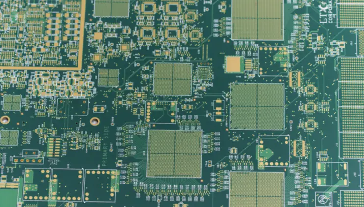
Display the plane layers one at a time and look for narrow necks rather than isolated clearances. Trace the return current path of each critical net on the layer it actually uses, and mark where that path is forced sideways. Those two views, the copper width and the traced path, are what reference plane integrity actually means in a design review. Confirm that no long slot crosses a route carrying a fast edge. Then record the checks and the assumptions in the release documentation, so the next revision can tell whether a change to the stack-up or the fanout invalidated them. Keep those records with the rest of the design rule set so the next engineer starts from the same assumptions.
Where the design is handed to a fabrication and assembly partner, the same geometry also has to survive the process. Aspect ratio, drill capability and copper balance all constrain what the fanout is allowed to become, and those limits belong in the conversation before the pattern is fixed rather than after the first panels are produced. Drill capability and stack-up limits are set by the fabrication process, and they should be confirmed during board manufacturing planning rather than discovered at the first article. A layout that depends on a copper channel which the fabricator has to thin is not stable, and the discussion is cheaper while the design is still a file.
The habit worth building is simple. When you open a fanout area, switch off the signal layers and look at the planes. If the copper between the antipads looks like a lattice rather than a sheet, the channel is not continuous, and no spacing report will tell you so.
FAQ
Is a stitching via next to every signal via enough? It handles the signal that changes layers. It does not restore a plane cut by a dense array far from that via.
How much copper counts as a continuous channel? Enough that the return current can follow the trace without a forced detour. The geometric check answers this better than a fixed number.
Does this only affect very high frequency designs? The effect grows with edge rate. A design with fast edges is exposed even when the clock is modest.
Can the fabricator fix it? No. The pattern is set by the design. Process limits constrain the pattern; they cannot restore a channel the fanout removed.
Summary
Via density is a plane integrity question, not a hole spacing question. Check the combined antipad geometry on every reference layer, keep a continuous return path under each critical trace, plan BGA fanout channels before filling the area, and verify the marginal cases with analysis or measurement. Add the checks to the release record, then confirm with the fabricator that the copper the design relies on is copper the process can actually hold.