Core Board Power Design: Rails, Sequence and Copper
A core board built around a high performance applications processor is a power design problem wearing a digital costume. The device presents a dozen or more supply rails at different voltages and very different current levels, it changes its load in nanoseconds, and it requires those rails to appear in a specific order. The schematic looks like a processor with a power management chip attached. The board behaves like a power supply with a processor on the output.
The guidance below is written for that class of design: a processor with dedicated domains for its compute blocks, its graphics unit, its image pipeline and its peripheral interfaces, together with memory supplies and a set of low noise analogue rails.
The Rails and What Sets Their Current
Typical domains include a low voltage core rail that carries the largest current, a separate rail for the graphics or neural accelerator block, a memory rail whose exact value depends on the memory type, an interface rail for the image pipeline, and general purpose input output rails at one of two common voltages. Each of these is generated by the power management unit, which contains switching converters for the high current rails and linear regulators for the low noise ones.
The current each rail must deliver is not simply the sum of the device maximum currents. The processor applies dynamic voltage and frequency scaling, so the core voltage moves with the operating point, and the supply has to track a commanded voltage change quickly while staying within its tolerance. That is the requirement that decides the converter bandwidth, the output capacitance and the layout, not the steady state current alone.
Specifications Worth Writing Down
Three figures define whether the distribution is adequate. The output voltage accuracy states how far each rail may drift from its nominal value under all conditions, including the load transient. The transient response states how much the rail may move for a given rate of current change, which for a processor of this class can be of the order of an amp per microsecond. The ripple limit states how much high frequency content is tolerated on top of the regulated value.
Alongside those, the input supply has to be defined. A nominal five volt adapter is adequate for a lightly loaded board, while a configuration with multiple displays or heavy peripheral use may need a higher voltage input to keep the input current and the loss within reason. The total consumption target then becomes an acceptance criterion for the assembled board rather than a marketing number.
Copper, Vias and the Distribution Network
The current path is designed in copper, and it belongs in the layout review alongside the signal nets. The core region needs a wide pour, and the outer areas need enough to carry their share without a significant drop; using copper on both sides of the board in parallel is a straightforward way to halve the resistance of a given route. Where a supply changes layer, the transition has to carry the full current, which means a group of vias rather than one: a cluster of small vias in parallel is the usual solution, and the ground return needs a matching group so that the loop is not restricted.
Inner layer treatment matters as much as the surface. Removing the unused pad of a via on layers it does not connect to frees copper on the plane beneath, which allows a wider power neck and a lower impedance at the same time. On the memory supply pins, a crossed pattern of connections distributes the current more evenly than a single trunk and avoids a concentration at the last pin in the chain.

Decoupling Placement
Decoupling capacitor selection is decided by distance before it is decided by value. A capacitor placed on the opposite side of the board directly beneath the supply pin is electrically closer than one placed a centimetre away on the same side, and the return connection should be short and direct, with the ground via close to the component rather than at the end of a long trace.
The network is then built from a combination: bulk capacitance for the low frequency content, mid value ceramic capacitors for the middle of the band, and small value ceramic capacitors close to the pins for the high frequency content. Combining a larger and a smaller value at the same location is common, but the ratios and the package sizes should be chosen so that their self resonant frequencies overlap rather than leaving a gap. The power plane pair with its ground partner supplies the impedance at the frequencies where no discrete capacitor is effective, which is why a continuous pair beneath the device is part of the decoupling rather than separate from it.
Sequence and Reset
Power rail sequencing is part of the device requirement, not a preference. As a general principle the low voltage core domains are established before the higher voltage interface domains, and the device datasheet defines the permitted delay between them. The memory supply has its own requirement, and on designs using a rail whose voltage is adjusted at runtime, the sequencing has to account for the possibility that the rail is being changed while other rails are already valid.
The reset signal has to remain asserted until the last rail has settled, and then remain asserted for the minimum time the datasheet specifies before being released. Releasing reset early produces a device that boots intermittently and blames the software, an outcome the functional test should be designed to catch by verifying the sequence, and it is one of the few failures that a well designed test can catch by checking the sequence rather than the final state.
Layout Rules Worth Keeping
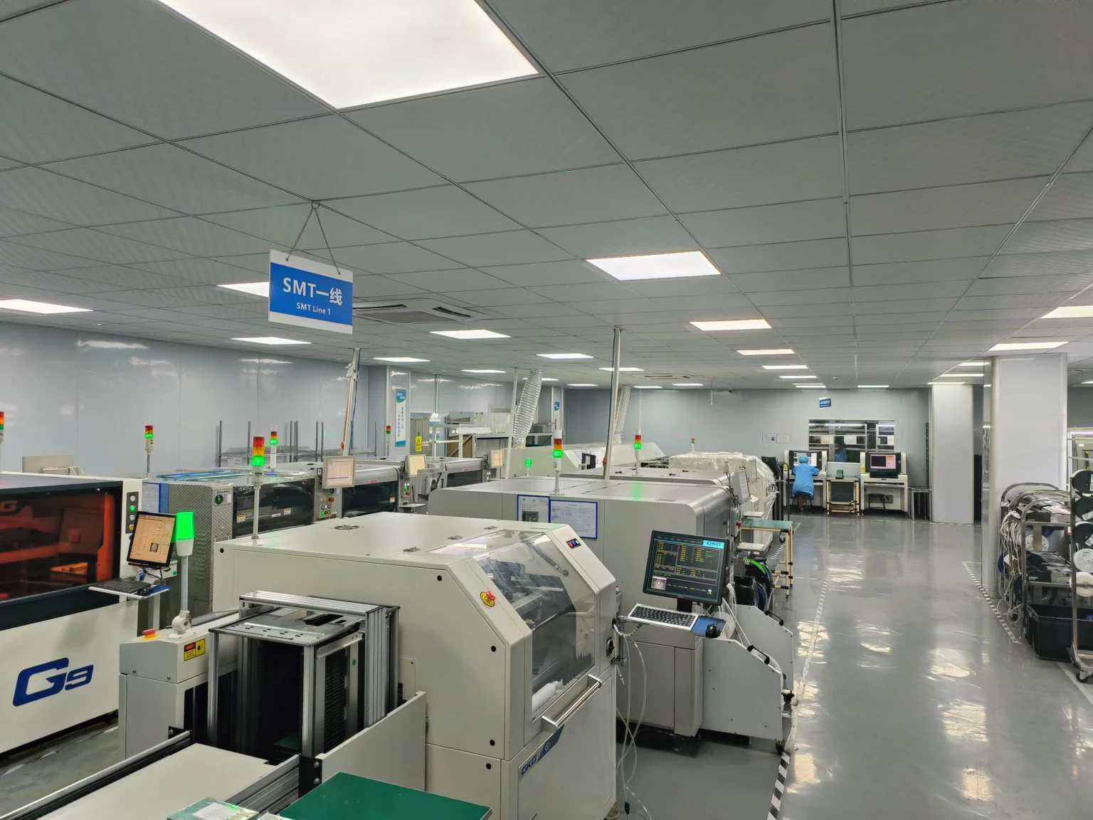
Keep switching converters and their inductors close to their output capacitors and away from the sensitive analogue area, and keep the switching node copper small. Enclose the sensitive modules with their own ground and place stitching vias at regular intervals around them. Where the power management device and the processor share a thermal path, the spacing between them is a compromise between heat spreading and the length of the traces between them, and the placement should be chosen with both in mind. Where the product is assembled by a partner, the thermal path and the paste deposit on a large ground pad are also assembly decisions, and they are worth reviewing with the assembly process owner.
Finally, confirm the copper that carries the current is copper the fabricator can actually produce, checking the capability before the stack-up is frozen. The trace widths, the via drills, the copper weight and the dielectric thickness all sit inside a process window, and a power distribution design that assumes a width outside that window will be adjusted by someone after the design is released. Agreeing the numbers with the fabrication partner while the design is still a file avoids the change.
FAQ
How many vias does a power layer change need? Enough to carry the current at an acceptable temperature rise, which is a calculation based on the via barrel, the copper and the current, not a fixed number.
Is a single bulk capacitor enough for the core rail? No. The impedance has to be low across the band the load excites, which requires several values and careful placement.
Does the sequence matter if all rails reach their final value? Yes. The device specifies an order, and a wrong order can leave it in an undefined state even when the voltages are correct.
What should the acceptance test check? The rail accuracy under transient load, the ripple, the power-up sequence and the reset timing.
Summary
Core board power design comes down to four things: define the rails and the transient requirement they must meet, build a copper and via structure that carries the current without dropping it, place decoupling where the electrical distance is shortest, and honour the sequence and reset timing the device specifies. Treat the power distribution as a designed subsystem rather than an attachment, and the board will boot the first time.