Backplane Design: Thick Boards, Press-Fit Connectors and Stubs
A backplane is the board that connects everything else. It carries little or no active circuitry, it is often the thickest board in the system, and it is expected to survive being assembled once and then working for a decade. Designing one is therefore a different exercise from designing a processor board: the electrical problem is dominated by connectors and stubs, and the mechanical problem is dominated by thickness.
The rest of the system is made of daughter cards inserted into the backplane, along with a power board and, usually, a card that does the housekeeping no one else wants.
What the Rack Format Imposes
Rack based equipment is built around a standard width and a repeated vertical pitch, with cards plugged into a chassis that also provides cooling and mechanical support. The backplane sits at the rear, carries the connectors for every slot, and provides the interconnect between them. Early designs were little more than connectors joined by traces; modern ones add power distribution, management signals and high speed links between slots.
The layer count on such a board can be high, because the number of connections is high and because the board has to route between slots that may be a long way apart. The thickness that comes with those layers is what makes the rest of the design unusual.
Thickness Changes the Connector Choice
The press fit connector is standard on boards of this class, and it is chosen for the assembly process rather than for cost. They do not require soldering, which matters because the thermal mass of a thick backplane makes it difficult to preheat and reflow reliably, and they allow a connector to be replaced or a board to be reworked without the risk of damaging the plating in a plated through hole.
The alternative, a through hole connector with a solder joint, runs into a mechanical limit. On a thick board the pin may not protrude far enough on the far side to form a reliable joint or to be reworked, and the solder process itself becomes difficult because the copper that carries the heat away is generous. The same copper is deliberately used elsewhere in the stack to raise the thermal capacity, which only makes the assembly problem worse.
The Stub Problem Is Worse Here
A signal entering from a connector often needs to reach an inner layer rather than the far side of the board. On a twenty layer board, a via that stops at layer four leaves a barrel extending through the remaining layers, and that unused portion behaves as a stub. At the frequencies used by modern backplane links, the stub resonates, and the effect on the insertion loss appears as a notch that closes the eye.
The remedy is to remove the stub after plating by drilling a slightly larger hole back to the layer where the signal exits. The operation costs an extra process step and requires control of the drill depth, but the improvement in the eye diagram is measurable, and on a link that runs the length of a chassis it can be the difference between passing and failing. The stack-up that makes it possible is a fabrication discussion. The alternative is a stack-up that places critical layers near the surface so the stub is short enough to ignore, which is a decision taken when the stack-up is defined rather than when the routing is done.
Power and Signal in the Same Chassis
A backplane carries the supply to every slot, and the currents can be large. The power distribution has to be designed as a network rather than as a set of wide traces: the copper, the connector pin assignments and the number of pins reserved for the return all determine the drop that each card sees, and the pin assignment determines the loop inductance that a card has to work with.
The separation between the power hardware and the signal path is the second consideration. A dedicated power board is common, because the switching circuits, their inductors and their heat can then be kept away from the sensitive part of the system. Where the two share a board, the shielding and the physical distance between them become part of the design review rather than an afterthought.
Partitioning the System Into Cards
The way a system is divided into cards follows the block diagram, but the divisions should also follow the technology. A module that needs a high layer count and fine geometry should not share a board with a module that would work on four layers, because the whole board then inherits the most expensive requirement. Grouping functions by their routing density, their power domain and their thermal needs produces a system that is cheaper to build and easier to revise, and the layer stack that results is easier to match to the fabricator capability.
Standardisation is the other consequence of a multi card system. A daughter card that follows an agreed electrical and mechanical interface can be replaced, upgraded or supplied from more than one source, and the backplane only has to provide the connector and the interconnect. Where that discipline is absent, every card becomes a custom design that has to be revised whenever the system changes.
Design and Assembly Notes
On the fabrication side, the aspect ratio of the holes, the drill capability for a press fit pin, the depth control for back drilling and the flatness of a thick panel all have to be confirmed with the supplier before the design is released. These are not numbers that can be adjusted after the fact without changing the electrical result.
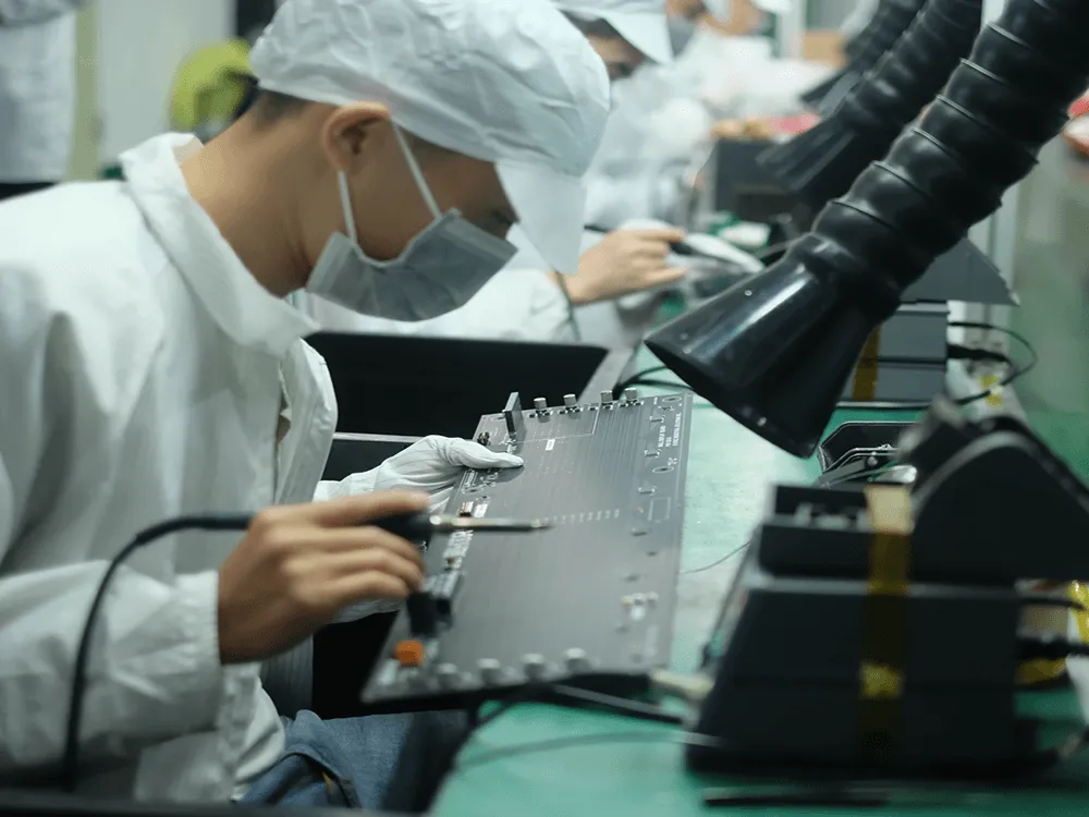
On the assembly side, the connector insertion process has to be defined: the force required, the support the board needs to avoid flexing, and the inspection method that confirms every pin is seated. A press fit pin that has not fully entered its hole may still make contact at room temperature and fail after a thermal cycle, so the inspection step is part of the product rather than an optional check. Where the board also carries surface mount components, their placement and the reflow profile have to accommodate the thermal mass of the board, and that is a conversation to have with the assembly partner during the design rather than after the first article. Connector seating is also a test step that should be defined and recorded.
FAQ
Why are press fit connectors used on backplanes? Because they avoid a solder process on a high thermal mass board and allow rework without risking the plated barrel.
Does every via need back drilling? Only where the remaining stub is electrically significant at the data rate of the link it carries.
Can a backplane be built on a thin stack-up? It can, but the mechanical stiffness required by a large connector array usually implies a thicker board.
What should be checked first? The connector interface and the stack-up, because both constrain everything that follows.
Summary
Backplane design is dominated by thickness and by connectors: press fit interfaces instead of solder, stub control through back drilling or a well chosen stack-up, power distribution sized for the pins and the copper available, and a system partitioned so that each card carries only the technology it needs. Settle the mechanical and interface questions first, and the routing becomes a familiar exercise on an unusually thick board.