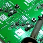
QFN Assembly and X-ray Inspection on a Charging Module Board
A charging module control board combines power management, sampling, communication and protection, and it usually carries both bottom terminated devices and a dense population of small passives. On a QFN assembly the visible fillets on the outer leads prove very little: they can look correct while the centre pad and parts of the perimeter have not formed a reliable joint. The stencil design and the post-reflow inspection have to be planned together for that reason.
Confirm the Package and the Pads First
The import package contains the Gerber data, the bill of materials, the placement coordinates, the assembly drawing, the quantity and the expected lead time, and where programming or functional testing is included it adds the program file, the supply range, the interface definitions, the test steps and the acceptance criteria.
The first check is a comparison: the part number of the device against the package size, the pin one orientation and the pad geometry on the board. Devices with similar names can differ in body size, in the dimensions of the bottom pad and in the lead pitch, so a discrepancy between the bill of materials and the Gerber data has to be resolved before the order runs rather than judged by eye at the machine. Where a substitute is permitted, the model number and the key parameters belong in the approval, not only the package name.

Evaluating the Stencil Aperture
The centre thermal pad is where the process is decided. If the stencil aperture over it is a single opening of the full pad area, the deposited volume is usually too large, and during reflow the device floats on the solder and tips slightly, which produces uneven wetting on the perimeter leads. If the opening is too small, the volume is insufficient and the connection under the body is weak.
The usual answer is a windowed aperture, in which the centre pad is covered by a group of smaller openings. The arrangement increases paste release from the stencil, distributes the solder more evenly across the pad and leaves channels for flux volatiles to escape during reflow rather than being trapped under the device.
The evaluation uses three inputs rather than one: the recommendation in the package data, the actual pad on the board and the customer requirement for the joint. A design with a large ground pad connected to internal planes also needs the thermal connection considered, because a pad that draws heat away quickly behaves differently from one that does not.
Printing and Loading
The printing stage depends on three conditions being right: the stencil cleaned at an interval suited to the aperture area, the board registered correctly, and the support arranged so that the board does not deflect under the squeegee.
After printing, the deposit is checked for area, volume, offset and bridging. If the perimeter pads of a QFN are consistently short of paste, the causes to investigate are the aperture release, the squeegee parameters and blocked apertures. The check happens before placement, because the same defect corrected afterwards is a rework operation on a board that may not survive it.
At loading, the reel labels, the orientation and the station positions are verified. The orientation of a QFN is confirmed from the pin one marking and the package marking rather than from the outline, because the body of a QFN often has no lead pitch to indicate rotation visually, and a part rotated by ninety degrees can look plausible on a board of the same size.
<img src="https://www.gopcba.com/wp-content/uploads/2026/08/43cb5004e0dfbd68a2cd4947418c747d.webp" alt="windowed stencil aperture over a QFN thermal pad” />
Inspection After Reflow
Optical inspection covers component offset, polarity, tombstoning, bridging and the joints that can be seen. The joints under a QFN are a different case, and X-ray inspection is used where the customer requirement and the risk in the design call for it.
The value of an X-ray image depends on the criteria being written down before the inspection. The items to specify are the acceptable void fraction under the centre pad, the permitted offset of the device relative to the pad, the presence of bridging between adjacent leads and the uniformity of the solder under the perimeter. An image without criteria is a picture; with criteria it is a measurement that can be compared between batches.
The image also has to be interpreted with the package structure in mind. A void pattern that is normal for a large centre pad with a grid of solder areas is a defect in a package with a different internal structure, and the difference is a property of the design rather than of the process.
Attributing a Defect
When an anomaly is found, the analysis works through the candidates in order: the paste deposit, the placement position, the incoming component, the board support and the reflow conditions. Each of those produces a different corrective action, and changing more than one at a time removes the ability to know which of them mattered. The X-ray image is the starting point for that analysis rather than the end of it.
Our SMT assembly process applies the sequence above to bottom terminated devices, and where the investigation identifies a cause that belongs to the design, such as a thermal pad that is too large for the stencil to release from or a pad with no thermal relief, the correction follows the same route as any other change in our design review. The results and the criteria applied are retained with the build in our quality management system.
Records and Traceability
The build is only repeatable if the conditions that produced it are recorded. For a bottom terminated device the record that matters includes the stencil revision and the aperture dimensions, the paste type and the printing parameters, the placement program revision, the reflow profile and the reflow oven used, the X-ray images with the criteria they were judged against, and the disposition of any board that was set aside.
That record serves two purposes. When a batch is questioned later, it shows what the process was at the time rather than what it is believed to have been, and when the same product is built again it gives the next run a starting point that has already been proven instead of a set of parameters to guess at. Where a change is made, the reason for it is worth recording too, because a parameter that was adjusted for one batch and carried forward without explanation tends to be treated as arbitrary later on.
For charging products the same records support the customer’s own traceability requirement, and for a build that includes programming and functional testing they connect the assembly result to the test result. Our industrial PCBA and PCBA testing services retain these records with the build.
FAQ
Why does a windowed aperture help? It releases paste more cleanly, distributes solder across the pad and gives flux volatiles a path out from under the device.
Is X-ray needed for every QFN? The requirement depends on the design and the customer specification. Where the joints are hidden and the product is safety or reliability relevant, it is normally specified.
What is the most common cause of a QFN that will not sit flat? Too much paste on the centre pad, which lifts the body during reflow and leaves the perimeter joints uneven.