Half-Hole and Stamp Hole PCB Manufacturing
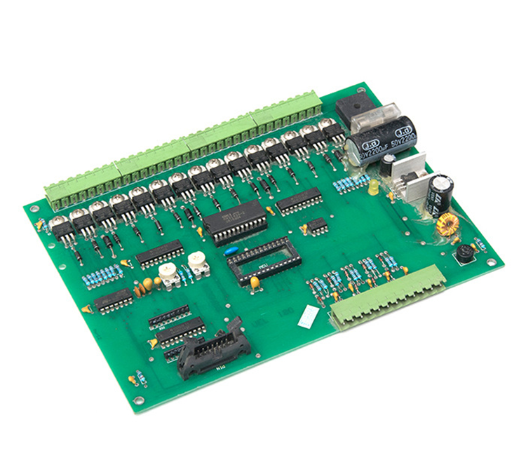
A module board that has to be soldered flat onto a mother board needs a connection that takes little space and carries the current without a connector in the way. The half-hole process is the usual answer. Two boards are joined by a row of plated holes, the outline is milled through the middle of that row, and each board keeps half of every hole along its edge. The result looks like the perforated edge of a postage stamp, which is why the boards are called stamps, and the connection is made by soldering the board edge directly to a matching pad on the carrier.
Where the Process Is Used
Radio modules for Bluetooth, wireless networking and cellular data are the most familiar case, because the module is soldered onto the main board and the joint has to be both compact and reliable. Power modules such as DC to DC converters and charging boards use the same edge to carry a larger current than a pin header of the same footprint would manage.
Sensor boards are built in panels and separated afterwards, and each small board keeps its half holes along the edge for the later soldering operation. Core boards and carrier boards form another group, where the core board is mounted vertically or flat onto the base board through the half holes, which removes the connector cost and improves both the signal path and the resistance to vibration.
The process is described by a number of names. A castellated hole is the general term for the plated half hole itself, while the stamp hole name comes from the appearance of the separated panel. Both refer to the same feature, and the difference between a half hole and a perforation used only to break the panel apart is worth stating clearly in a drawing, because they are not the same requirement.
Where the Difficulty Lies
Milling through the centre of a plated hole is what makes the process demanding. The copper in the barrel is cut on one side and left on the other, and if the cutting direction and the tool parameters are not controlled, the copper lifts and forms a burr or a strand that interferes with soldering and with the appearance of the board.
The position of the cut is the second issue. The mill has to follow the centre line of the hole, because an offset leaves one side with more copper than the other and produces a joint that varies along the same edge. Optical positioning and a forming machine that holds the tolerance keep the cut where it belongs.
The third issue is the panel design. The connections between the boards, the path the tool follows, and the direction in which the material is stressed all affect the yield. A panel that is easy to rout may be difficult to hold flat while it is being routed, and a panel that holds flat may put the stress of separation where the copper has already been weakened. Our engineering group reviews the design at the CAM stage and returns comments before the panel is released.
Design Rules Worth Following
The half hole diameter is normally kept at nought point five millimetres or more, and the centre of the hole is placed at half the diameter from the board edge. Copper is left around the hole so that the pad does not come away while the edge is being cut. Keeping the holes aligned in one direction makes the routing simpler, and keeping them away from the corners avoids the region where the panel accumulates stress.
Where the design intent is not clear, the Gerber data can be reviewed before the order is placed. A review at that stage costs a conversation and may save a panel, which is a better trade than finding the problem after the boards have been milled.
Capability and the Production Flow
Rigid boards from two to sixteen layers are produced in this process, with thicker and higher layer count panels evaluated individually. The finished thickness runs from nought point six to two point four millimetres, the surface finish can be hot air levelling, immersion gold or OSP as the product requires, and a single piece can be ordered so that the prototype and the production lot follow the same route.
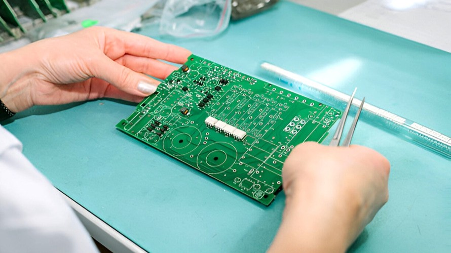
The flow begins with cutting and inner layer work, where a multilayer panel is laminated after its inner layers are formed. Drilling and plating follow, which establishes the copper thickness in the barrel. The outer pattern, the soldermask and the legend come next, then the surface finish, and only then the forming operation that cuts along the centre of the hole row. Inspection of the half hole appearance, of the barrel and of the burrs follows, and the electrical test and packing close the order.
Standard lead time is three to seven days, with an expedited route for simple double sided panels. Our PCB manufacturing group runs the process and the review, and the panels can continue into SMT assembly at the same site when the module also has to be populated.
Soldering the Module to the Carrier
The joint is made by reflowing solder paste on the carrier pads and placing the module edge onto it, so the paste volume and the pad geometry on the carrier decide the result. A pad that is too short leaves a fillet that starts and ends abruptly; a pad that is too long spreads the solder away from the edge. The carrier footprint is designed with the module edge in mind rather than copied from a header pattern.
Modern coatings on the tip can help a first prototype, but the assembly that goes into production is soldered with paste and reflow, because a hand soldered edge is not repeatable across a batch and cannot be inspected from the side. Where the module is a module board that carries its own shielding, the shield has to be fitted after the edge joint, or the nozzle of the reflow oven will not reach the edge at all.
Inspection of the finished joint uses the visible fillet on the outside of the edge, and where the carrier is a multilayer board with an internal plane connected to the edge pads, the thermal mass of that plane changes the profile that the joint needs. Our SMT assembly group handles the carrier build and this edge soldering as one operation.
FAQ
How much more does a half hole board cost? The forming operation and the additional inspection add to the price of an equivalent plain board, and the difference depends on how many half holes the design carries. Against the cost of a connector, the comparison usually favours the half hole.
How small can the half hole be? Nought point five millimetres is the usual minimum. A smaller hole raises the risk of lifted copper and of position error, and it is evaluated case by case.
Is a half hole the same as a perforation? No. A perforation only breaks the panel apart, while a half hole is plated and is soldered afterwards. The drawing has to say which one is required.