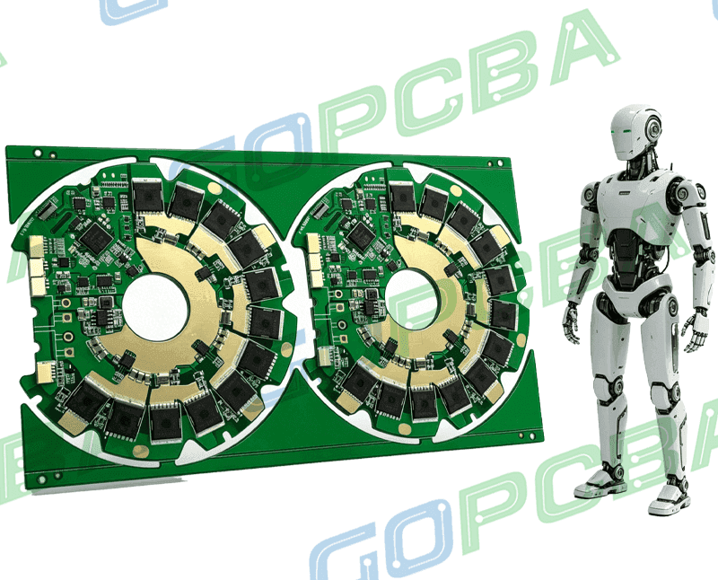
Heavy Copper PCB Manufacturing From 3oz to 6oz
Power modules, industrial drives, energy storage and automotive systems all carry currents that a conventional board with one ounce of copper cannot handle. Increasing the thickness of the copper is the direct answer: for the same width of trace, more copper means more current, less conduction loss and less heat, and in some designs it also improves the ability of the board to spread heat and to resist mechanical stress.
Where It Is Used
Power modules and switched mode supplies are the clearest case, including direct current converters and power amplifiers. Industrial control equipment follows, with drives, servo controllers and high power control units. Energy applications include battery management boards, charging equipment and photovoltaic inverters, and automotive applications include on board supplies, motor drives and battery management.
A current carrying calculation is not a matter of the copper thickness alone. The width of the trace, the permitted temperature rise and the cooling available all take part, and the thickness and the width are chosen together from the actual current and the limit on temperature. Our design group works through that assessment with the customer and recommends a copper weight and a routing that satisfy it.
Capability
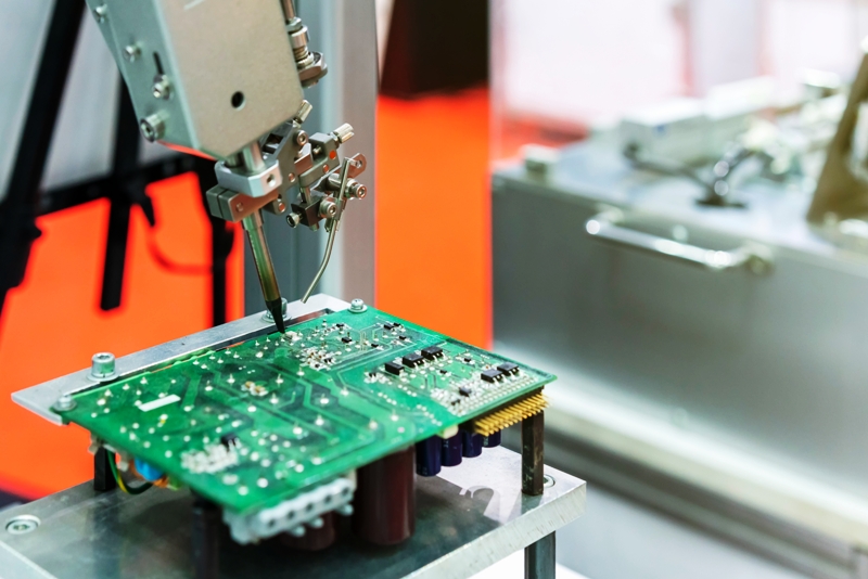
Heavy copper boards are produced with an inner layer copper weight of three to six ounces, with the outer layers set according to the process conditions of the particular design. The layer count runs from two to twenty on multilayer heavy copper work, and the finished thickness is normally between one point six and three millimetres depending on the copper and the number of layers. The minimum trace width and spacing follow the copper weight, and at three ounces the figure is around five thousandths of an inch. Ordinary FR4 is used in most cases, with a high glass transition temperature grade where the product runs hot, and the surface finish is chosen from hot air levelling, immersion gold or OSP according to the conditions. Acceptance follows the IPC-A-600 standard.
What Makes the Process Difficult
Lamination is the first difficulty. A thick copper foil and a resin system with different rates of thermal expansion do not move together, and the board has a tendency to bow. The stack-up is made symmetric, the prepreg arrangement is planned deliberately, and the pressing parameters are adjusted, after which the flatness of the finished board is measured. Keeping warpage inside about nought point seven five percent on a one point six millimetre board satisfies most assembly requirements.
Etching is the second. The thicker the copper, the longer the etchant has to act, and the longer it acts the more it removes from the sides as well as from the top. That sideways removal narrows the trace and changes the profile, so the parameters and the compensation factors are adjusted to keep the line width inside the tolerance the current requirement needs. This is one reason the minimum width is larger on heavy copper than on an ordinary board.
What the Current Figures Look Like
The approximate figures below are for an inner layer trace under natural convection cooling, and they are a starting point rather than a design rule. One ounce of copper, roughly thirty five micrometres, carries about five amperes at a ten degree rise and about seven at a twenty degree rise, which suits signals and small power circuits. Two ounces carries about eight and about eleven, and suits ordinary power boards and small power modules.
Three ounces, roughly one hundred and five micrometres, carries about eleven amperes at ten degrees and about fifteen at twenty, which covers high current supplies and industrial drive boards. Four ounces reaches about thirteen and about eighteen, which suits larger power modules and energy components. Six ounces, roughly two hundred and ten micrometres, carries about seventeen and about twenty three, which is the region of very high current and power electronics equipment.
<img src="https://www.gopcba.com/wp-content/uploads/2026/08/773604150_122204755928591289_8347654747047466302_n.jpg" alt="thick copper traces on an inner layer after etching” />
Why the Figures Are Only a Starting Point
The actual capacity of a trace depends on the material, the layer count, the cooling conditions and the length of the path as well as on the copper. A trace in an inner layer with copper planes above and below it behaves differently from one on an outer layer in still air, and a short trace that connects to a large pad conducts heat away into the pad. A trace carrying a high current into a connector also depends on the connector, which is often the real limit.
Where the margin is thin, the assessment is confirmed with a simulation or with a measurement on a test board rather than taken from a table. The extra step is much cheaper than a board that runs hot in the field, and it is the reason the design assessment happens before the artwork is released.
Working With the Design
Because the copper weight, the width and the stack-up are decided together, it is worth involving the fabricator while the layout is still being drawn. A stack-up that can be produced at three ounces may not be producible at six, and a trace width that was drawn for one copper weight is not valid for another. Finding that out after the artwork has been finished means the layout is redone.
Heavy copper boards also take longer to produce than an ordinary one ounce board, because the etching and the lamination each need more time. A two to eight layer board at three ounces is normally delivered in about seven to ten working days, and a six ounce or heavier board is quoted from its process difficulty. The estimate is given before the order is accepted rather than discovered during it.
The process sits alongside the rest of our capability. Production runs on boards from simple two layer work up to twenty layers, the design team can be involved in the current assessment and the stack-up planning, and the quality system holds ISO 9001 and IATF 16949 certification. Boards move into SMT assembly without being packed and reopened, and the design work is carried out by the same PCB design and layout group under quality management.
What to Send for a Quotation
`r`n
The Gerber data and the copper weight required on each layer are the essentials, together with the layer count, the finished thickness and the surface finish. Where a current requirement is the reason for the heavy copper, stating the current and the permitted temperature rise allows the width to be checked against the design rather than assumed.
`r`n
It also helps to say which traces are actually carrying the current. Applying heavy copper to a whole layer when only two traces need it increases the cost of lamination and etching for no benefit, and a design that keeps the thick copper where the current flows and uses ordinary copper elsewhere is cheaper to produce and no less capable.
FAQ
How much does the price rise between three and six ounces? Both the material cost and the process difficulty increase with the copper weight, so the price rises, and the amount depends on the layer count and the board area as well.
How narrow can a heavy copper trace be? At three ounces, around five thousandths of an inch is the practical figure, and the width capability falls as the copper gets thicker because the sideways etching increases.
Is heavy copper always warped? It is more prone to it than an ordinary board, which is why the stack-up symmetry, the pressing parameters and a levelling step are all used to control it.