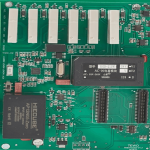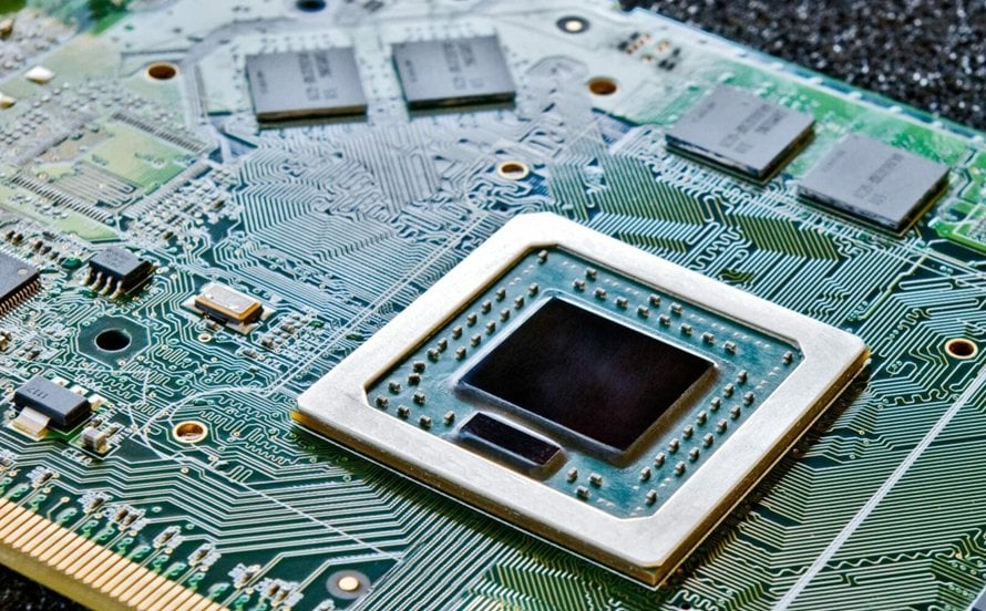
Micro Main Board Assembly for Wearable Devices
The main board in a wearable device fits in a small area and still has to carry a processor, sensors, memory, power management, charging contacts and a board to board connector. For a project like this the question is not only whether the machine can place the smallest package. It is whether the board can be printed on reliably, whether the connector stays flat, and whether the finished height fits inside the space the enclosure allows.
Can the Board Pass Through the Line Reliably
An irregular outline, a notch in the edge or a very small board is not well suited to being fed through the machine on its own. When the Gerber data are supplied, the board thickness, the panel arrangement, the separation method and the areas that are forbidden to the structure can be stated at the same time.
During import the process edge, the fiducials, the tooling holes and the support positions are checked. A thin board, or a panel with a large number of slots, may need a carrier fixture to prevent it from deflecting during printing and moving during transfer. The fixture must not cover a fiducial or press on a pad or a component on the underside, and where a wearable device board is assembled on both sides, the fixture also has to leave clearance for printing the second side.
<img src="https://www.gopcba.com/wp-content/uploads/2026/09/122.jpg" alt="wearable device main board in a carrier fixture” />
The Stencil Must Suit Both the Micro Pads and the Connector
A micro assembly usually carries small passives, a bottom terminated device, a sensor and a board to board connector at the same time, and they do not need the same volume of paste. The stencil aperture is therefore designed per feature rather than by scaling every opening by the same factor. The fine pitch of the connector means that excess paste produces a bridge, while a sensor or a device with a pad underneath needs coverage that is adequate enough to form a joint across the whole pad.
After printing, the area, volume, offset and height of the deposit are observed so that an anomaly can be intercepted before placement rather than found after reflow. If one region is persistently short of paste, the cause is a blocked aperture, the support under the board or the release of the paste from the stencil, and raising the reflow temperature to compensate is not a cure for a print that was wrong.
Beyond Placement Accuracy: Component Height
The customer supplies a complete bill of materials, the placement coordinates and the assembly drawing, and marks the connectors, sensors and low profile packages that must not be substituted. Two board to board connectors that look alike can have different mating heights, and a wrong one produces a joint that looks perfectly normal and an assembly that will not mate with the other board or fit the enclosure.
When the placement programme is written, the component angle, the nozzle, the vision recognition and the feeder packaging are all confirmed. After the first article, the orientation and the joints are checked together with the flatness of the connector, the height of the components and the position of the charging contacts.
Where the customer can supply the mating connector, a structural sample or a height limit, the first article can be tried against it. Verifying the assembly at that point is far cheaper than discovering the problem once the whole batch has been built.
Inspection After Reflow
After micro PCB assembly has passed through the oven, optical inspection covers the missing parts, the offset, the reversed parts and the visible joints. The pins of a small connector are closely spaced, so a magnified check is used to confirm the bridges and the state of the pins.
For a device with joints beneath the body, the extent of any further examination is agreed with the customer. Sensor testing, programming and charging interface verification follow the procedure the customer provides rather than being replaced by a simple power-up check, because a board that switches on has not been shown to measure or charge correctly.
Where a repair is needed, the heat is applied locally so that the neighbouring micro components do not move. A repaired board is inspected and tested again, rather than only the position that was worked on being examined.
Freezing the Structure and the Material Before Volume
A wearable board usually sees a number of changes during the prototype stage: a connector is exchanged, a sensor is moved, a height is adjusted. Before volume production starts, the Gerber data, the bill of materials, the coordinates, the programme and the assembly requirements are frozen, and the question of whether a temporary substitute continues to be used is decided rather than assumed.
Providing the board thickness, the structural height limits, the mating connector, the test requirement and the delivery date along with the production files allows the processing method to be chosen from the actual assembly conditions. Our SMT assembly lines handle the micro placement, internet of things PCBA covers the connected wearable flow, and PCBA testing runs the functional checks.
What the Order Data Should Include
`r`n
The production files are the Gerber data, a complete bill of materials, the placement coordinates and the assembly drawing. On top of those, a wearable project benefits from three pieces of information that are specific to the product: the thickness of the board, the height available inside the enclosure, and which connector or part of the assembly has to be verified for fit.
`r`n
Where programming is included, the programme file, the interface definition and the way the revision is read back are needed. Where charging or sensing is verified, the supply conditions, the battery and the acceptance criteria are needed, because a charging test carried out with a different battery or cable gives a different result on the same board.
`r`n
It is also worth stating the areas that must not be covered or occupied: a fiducial that has to stay visible, a contact area that has to remain clean, a feedthrough for the enclosure, or a region reserved for an antenna. Those constraints are cheap to respect when they are known and expensive to discover after the panels have been printed.
`r`n
Handling the Micro Components
`r`n
Components at the small end of the range demand more than a placement programme. The nozzle has to be in good condition, the feeder has to deliver the tape consistently, and the vision system has to recognise the part reliably. Where the same reel supplies a part to several stations, the loading is verified against the bill of materials so that two similar values are not mixed.
`r`n
Static control also matters more on a small assembly, since the insulating materials accumulate charge and a discharge can damage a device without leaving a mark. Handling is done with grounded wrist straps and conductive containers, and boards in transit are kept in antistatic packaging rather than in a plain tray.
FAQ
Why is a carrier needed for a small board? Because a thin or slotted panel deflects under the squeegee and moves during transfer, and the fixture keeps the print and the position stable.
Can one stencil serve all the components? It serves them, but the openings differ: fine pitch connector pins need less paste than a large pad underneath a device.
Why check the connector height on the first article? Because two similar connectors can differ in mating height, and the error only appears when the product is assembled.