AI Server SMT Assembly: Large Packages and Thermal Loads
Assembling an AI server board is different from assembling an ordinary control board, and the difference is not the number of components. It is the physical scale of the devices, the amount of heat they produce and the density of the connections beneath them. A single accelerator package can carry thousands of balls at a fine pitch, sit on a board with thirty layers and dissipate more power than the rest of the assembly combined. Each of those conditions constrains the process, and they interact with each other.
The Large Package and Its Placement
Placing a package of that size means handling a component whose mass is significant relative to the board and whose ball array has to align with a pad array across its whole area. The placement machine has to recognise the package accurately, since a small rotational error at the corner becomes a large linear offset at the opposite corner, and the placement force has to be controlled so that the balls are not deformed before reflow.
The board itself contributes to the difficulty. A thick, high layer count board with heavy copper planes is stiff, and a stiff board and a heavy package are more sensitive to any variation in the surface. Warpage that would be absorbed by a thin board becomes a gap between the package and the pads, and a gap of the wrong shape produces joints that differ across the array.
The thermal pad beneath the centre of the package is the critical feature. It has to receive enough paste to form a continuous thermal path and not so much that the component floats on a layer of alloy while the outer balls fail to contact. The stencil opening for that pad is divided so that the paste volume is controlled and the flux can escape during reflow.
Printing for a Board of This Shape
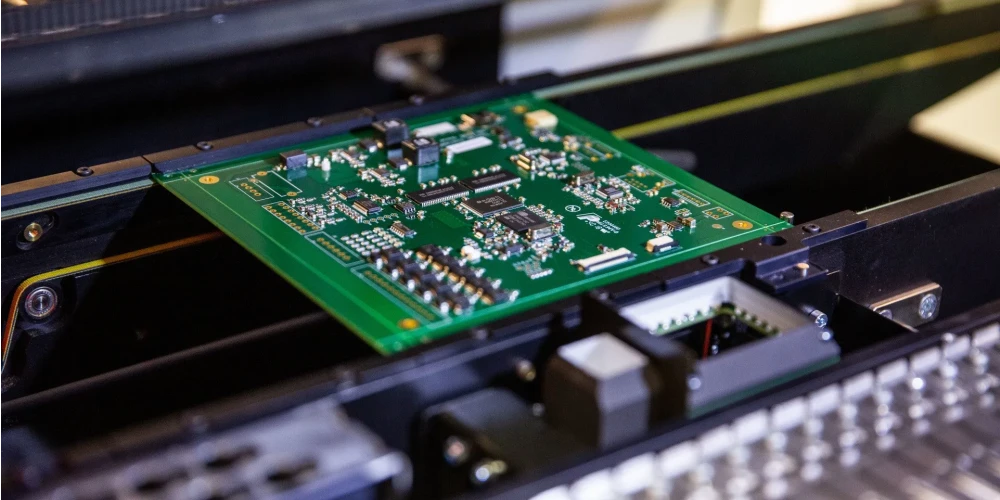
The paste deposit has to be consistent across a panel that is large and stiff, which places demands on the printer and on the support beneath the board. A support that leaves a gap allows the panel to flex, and the resulting variation in the deposit appears as a difference between one region of the panel and another. The paste inspection measures that variation directly and is the reason the print is verified rather than assumed.
The aperture design differs across the board because the requirements differ. The ball array needs openings that deliver a consistent volume to each pad; the thermal pad needs a divided pattern; the passive components around the package need ordinary openings at a smaller thickness than the array can tolerate. A stencil that treats the whole board as one geometry will produce defects in at least one of those regions.
The volume of paste consumed by a board of this class is large, and the state of the paste on the stencil changes during a run. The cleaning interval and the working life of the paste are therefore part of the process rather than incidental, and a run that is stopped and restarted leaves a stencil whose condition has changed in a way that affects the next print.
Reflow With a Large Thermal Mass
A board of this size holds a lot of heat and takes time to reach temperature. The thermal pad and the copper beneath it act as a heat sink during the ramp, so the assembly may reach the liquidus at the surface before the interior of the joint is ready. The reflow profile is measured on the actual assembly with thermocouples placed beneath the package as well as beside it, because a profile that satisfies the board surface may leave the joint under the device short of temperature.
The soak is the stage that matters most in this case. It gives the assembly the time to equalise so that the small components and the large device reach temperature within a shorter interval of each other, which is what prevents the small passives from reaching the liquidus long before the package does.
Inspection and What Cannot Be Seen
The ball array is beneath the package and cannot be examined optically, so the inspection combines the optical check of the visible periphery with an X-ray image of the array. The X-ray shows the arrangement of the balls, the presence of bridges between them and the shape of the joints, and it is interpreted against the structure of the package rather than by a fixed rule applied to a grey scale.
A package of this size also makes rework a decision rather than a routine. Removing and replacing it applies a large thermal cycle to a board that has already been reflowed, and the surrounding components are exposed to the same cycle. The X-ray result, the functional test and the cost of a new assembly are compared before the decision is taken, and in a significant number of cases the answer is to build a new board rather than to repair one.
The test stage has to be prepared to match. A board of this scale requires a fixture that supports it, contacts that do not disturb the packages and a supply capable of the current the device draws. Bringing that fixture up in parallel with the production preparation is what allows the first assembled batch to be tested rather than stored. Our assembly operation handles this class of product through SMT assembly and high volume PCB assembly, the boards come from PCB manufacturing, the fixtures and the electrical checks sit under PCBA testing and the records are held with quality management.
Planning the Run Around One Device
On a board of this class, the production planning is effectively organised around the largest device. The stencil, the profile, the placement programme, the inspection programme and the test fixture are all shaped by the requirement of that one package, and the smaller components are placed within the process window that the package defines rather than the other way around.
That has a practical consequence for scheduling. The product cannot be run on any line, because the placement machine has to be capable of the package, the printer has to handle the panel, the oven has to deliver the profile and the X-ray facility has to be available for the array. The line is identified in advance and the product is planned against it, which is why an abrupt change of quantity on an order of this type is harder to absorb than on an ordinary board.
The material planning follows the same logic. The large devices are expensive, they carry long lead times and they are supplied in packaging that is sensitive to moisture and to mechanical damage. They are received and stored under controlled conditions, the exposure time before reflow is recorded, and a reel that has been opened longer than permitted is dried before use rather than used on the assumption that it will be acceptable.
What the Customer Should Expect
A customer placing a board of this type should expect the process to be developed rather than applied. The stencil is designed for the specific device array, the profile is measured on the actual assembly, the inspection programme is written for the package and the fixture is built for the board. Those are the activities that consume the time before the first unit is produced, and they are the reason the lead time is longer than for an ordinary assembly.
The customer should also expect to be involved in the review points. The footprint, the thermal pad geometry, the panel arrangement and the test access are all decisions where the customer’s knowledge of the device and the supplier’s knowledge of the process meet, and a decision taken by one side alone is frequently not the best one available. Supplying the manufacturer’s land pattern recommendation together with the device specification shortens that conversation considerably.
FAQ
Why is the thermal pad opening divided? To control the paste volume and to let the flux escape, so the component settles onto its pads rather than floating on alloy.
Why measure the profile beneath the package? Because the board surface can reach temperature while the joint under a large device has not, and only a measurement inside the array shows it.
Is rework practical on a large package? It is possible but expensive, and the comparison against building a new assembly frequently favours the new assembly.