QFN Soldering and BGA Placement: Control Before Inspection
On a board using QFN soldering and BGA placement, most of the joints are underneath the component and cannot be seen after reflow. That single fact changes the shape of the process. Quality cannot be inspected into the assembly at the end, because the end of the process is the point at which the joints disappear; it has to be controlled from the data review, through the stencil and the print, to the placement and the thermal profile.
The failure modes are well known — bridging under a lead, insufficient solder, voids and an open joint that only appears under load — and each of them has a stage in the process where it is cheaper to prevent than to find.
Checking Pads and Material Before the Run
An order of this type starts with the fabrication data, the bill of materials, the placement coordinates, the assembly drawing, the quantity and the date. The bill of materials should state the complete part number and package for every QFN and BGA device, and the assembly drawing should carry the orientation, because the legend printed on the board is not a reliable substitute for a drawing.
Where the fine pitch devices are customer supplied, the original packaging, the moisture sensitivity label and the material information are retained. Whether a package has been opened, how long it has been exposed and whether it needs treatment before reflow are questions that must be settled before the parts reach the machine rather than afterwards.
The pad design is reviewed in the same pass: pad dimensions, solder mask openings, the thermal pad and the via arrangement beneath it. A thermal pad opening that is too generous concentrates paste and can lift the body; one that is too small restricts heat transfer and weakens the joint. Both are design issues that can still be corrected before production, which is the only moment at which they are cheap.
Stencil Openings for a Thermal Pad
A QFN has fine peripheral lead spacing and, in most cases, a large thermal pad in the centre. The stencil opening has to satisfy both. The peripheral apertures are sized to deliver enough solder for a reliable fillet without risking a bridge, while the centre is often divided into a grid of smaller openings instead of one large one, so that the paste does not gather into a single mass that lifts the part when it reflows.
The division also affects voids. A paste deposit that traps flux volatiles under a large pad produces voids that show up on X-ray and reduce the thermal path, and a windowed or segmented opening gives the volatiles somewhere to escape.
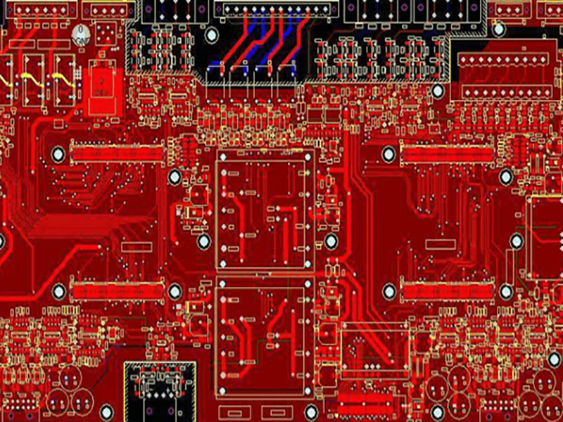
Print Control With Solder Paste Inspection
After printing, solder paste inspection measures the height, area, volume and offset of each deposit. A run of consistently short deposits, a localised surplus or a systematic offset is a signal to stop and correct the stencil, the squeegee, the board support or the printer settings — not a signal to place the parts and rework later.
This is the stage at which the economy of the whole process is decided. Correcting a print problem costs a few boards and a few minutes; correcting it after reflow costs the devices, the board and the time, and on a BGA it may cost the board as well.
On small batches the first article carries more weight than it does in a long run, because there is no volume in which a trend can be seen. The first board is checked for device orientation, placement position and print result, and the small packages around the fine pitch devices are checked for displacement before the run continues.
What BGA Placement Requires
BGA placement depends on the recognition, the pick and the positioning stability of the machine. The package, the ball array orientation and the rotation angle in the coordinate file are confirmed against the assembly drawing before the run, because a mismatch between the data angle and the direction the machine recognises produces a device that is placed perfectly and rotated by ninety degrees.
After placement, the body is checked for displacement or rotation on the first board. A device that has shifted on the paste is a print or placement pressure problem, and it is worth resolving before the rest of the batch is built rather than after.
Reflow That Suits the Whole Board
The thermal profile is set for the assembly, not for the fine pitch device alone. Board thickness, copper distribution and the other components on the board all take part: a connector, an electrolytic capacitor or a component with a low temperature limit can constrain the peak that the rest of the board would happily accept.
The profile is confirmed against the first article rather than assumed from a previous product, because a heavier board or a denser layout changes the way heat arrives at the joints underneath a package.
What AOI Sees and What X-Ray Adds
Optical inspection finds missing devices, displacement, reversal and visible joint defects, and it is the right tool for the peripheral joints it can see. It cannot see under a BGA, and for the joints beneath a QFN it sees only the fillet at the edge of the pad.
Where the customer specifies it, or where a device with hidden joints performs a critical function, X-ray is added. It shows ball connections, bridging and voids, and it turns an invisible joint into a visible one. The service is arranged through PCBA testing, while the assembly controls live with SMT assembly, the inspection criteria with quality management, the material with component procurement, and any pin-in-hole parts on the same board are handled through through-hole assembly.
Finding the Cause of an X-Ray Anomaly
An X-ray image is evidence, not a verdict. A single frame that appears to show a void or a bridge is interpreted together with its position on the board, the results of the functional test and the behaviour of the rest of the batch. A defect that appears at the same joint on every board points back to the stencil opening, the pad design or the print condition; a defect that wanders points towards material state, placement or the thermal profile.
After the fine pitch and array devices are placed, the board continues through any pin-in-hole operations, programming and functional test. When a board fails, the fault is traced back through the hidden joints, the peripheral circuit, the material and the programme before it is attributed, and a board that has been reworked goes through the full test again rather than the test it failed.

Records That Make the Process Repeatable
The settings that produced a sound batch are worth more than the batch itself, because the second order is where they pay back. The stencil, the print parameters, the machine programme, the placement data and the thermal profile are recorded together with the first article result, so that a repeat order begins from a known point rather than from a fresh investigation.
Where a defect was found and corrected, the correction belongs in the record as well. A stencil that was revised, a support pin added beneath a BGA, an offset applied to a coordinate — each of them is a small piece of knowledge that stops the same fault from reappearing when the product is built again by a different operator on a different shift.
That continuity is also what makes the inspection stages meaningful. A measurement is only comparable when the conditions under which it was taken are known, and an X-ray result from six months ago can be interpreted only against the settings that produced it.
FAQ
Why is inspection alone not enough for a BGA? Because the joints are beneath the package, so the process has to be controlled at printing, placement and reflow, where the faults can still be prevented.
What does solder paste inspection add? It measures the deposit before the device is placed, which is the last point at which a print problem can be corrected at negligible cost.
When is X-ray required? Where the customer specifies it or where a hidden joint performs a critical function; otherwise optical inspection covers the visible joints and the rest is confirmed by functional test.