




High-Frequency Material Systems and Lamination Control
When a design moves into the range where signal behaviour matters, the board stops being a mechanical support with copper on it and becomes part of the circuit. The dielectric properties of the material, the geometry of the traces and the way the layers are pressed together all influence how a signal arrives, and the fabricator’s control of those variables becomes part of the electrical performance of the product.
Building with a high-frequency material is consequently a different exercise from building with the standard grades, and the differences are concentrated in the material system, the lamination and the measurements that prove the result.
The Material System and What It Changes
The resin, the reinforcement and the copper foil form a system, and each of the three has a version intended for high-speed work. The resin is chosen for a low dielectric constant and low loss, the reinforcement for consistency of the dielectric properties across the panel, and the foil for a smooth surface, since a rough surface increases the loss at high frequency.
Those characteristics are what allow the impedance of a trace to be predicted from its geometry, which is the basis on which a high-speed design is dimensioned. Where the properties vary across the panel, the impedance varies with them, and a design that was simulated with one value behaves differently in production.
Substituting within this system is therefore a design decision rather than a purchasing one. A material from a different family may meet the description in general terms and still change the dielectric constant enough to shift the impedance, which is why the stack-up and the approved alternatives should be agreed in writing before the panel is built.
Working With These Materials
The materials behave differently in the process, and the differences are not always obvious from the data sheet. Their thermal expansion and their response to pressure and temperature in the press differ from the standard grades, and the parameters that suit one family do not transfer directly to another.
Some of them are also less cooperative mechanically. Materials that achieve their electrical performance through a particular filler or a particular resin chemistry can be more brittle, and the drilling and the routing have to be adapted accordingly, with the tooling changed more often to preserve the hole quality.
Adhesion is a third area. Where a material is inherently less receptive to plating, the preparation of the surface before the copper is applied becomes a process step that decides whether the connection to the inner layers is reliable.
Lamination and Layer Registration
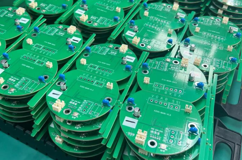
On a dense board the press is where many of the final properties are decided. Each lamination cycle applies heat and pressure, and each one moves the layers slightly. With a small number of layers the accumulated movement is tolerable; with many, the registration of an inner layer relative to its neighbours becomes a quality variable in its own right.
The consequence of poor registration is not only a mechanical misalignment. The distance between a trace and the reference plane beside it changes, and with it the impedance. On a board where those distances were calculated, a shift of a few tens of micrometres is an electrical error as well as a dimensional one.
The other variable in the press is the distribution of copper on each layer. A power or ground plane that covers most of its layer and a signal layer that covers very little behave differently under pressure, and the resulting flow of resin can leave an uneven thickness or, in the worst case, a void. Balancing the copper and allowing for the resin flow belongs in the design as well as in the process.
Where the specification requires it, a cross-section taken from a finished panel is the evidence that the lamination did what it was supposed to: the layer thicknesses, the registration and the copper geometry can all be measured from it.
Measurements That Prove the Result
The electrical requirements are verified by measurement rather than by inspection. Coupons built into the panel provide a trace whose geometry is known, and its impedance is measured and recorded against the target.
Those measurements should be attached to the delivery, since they are the evidence that the electrical intention was realised. A report that states the results, the target and the sample on which they were taken is comparable between batches; a statement that the boards passed is not.
<img src="https://www.gopcba.com/wp-content/uploads/2026/06/Juniper-Networks.png" alt="layer registration check on a laminated panel” />
Choosing a Fabricator for This Class of Board
The questions that establish capability are specific: which material families are held in stock and which are ordered, how many layers are produced routinely, what impedance tolerance can be held and measured, whether buried connections are made in house, and what the cross-section shows on a typical panel.
The distinction between possible and routine matters more here than on an ordinary board, because the process window is narrower and the accumulated experience of a material family is what keeps the results consistent. A fabricator who builds several projects a month in a given system has a different relationship with it from one who has tried it once.
The design data belongs at the front of the conversation. A stack-up that names the material, the thickness of each layer and the target impedance, together with the routing that has to meet it, allows the process to be planned instead of adjusted, and it is the document through which any question about a substitution can be answered. The assembly that follows is carried out as SMT assembly, with verification through PCBA testing and the controls under quality management.
Substitution and the Approval Behind It
Where a material is unavailable, the temptation is to treat the nearest equivalent as a formality. On a board of this class it is not, because the electrical behaviour is a property of the dielectric constant and the loss of the material as much as of the trace geometry drawn on it.
The way to keep the decision manageable is to agree the alternatives in advance. Where the designer names the materials that may be substituted, and the conditions under which the substitution is acceptable, the choice can be made by the fabricator without a new electrical review. Where the design depends on a single grade, saying so prevents a well-intentioned substitution from changing the impedance.
The laminate record belongs with the delivery for the same reason, and it is the one document that makes a comparison between two batches possible. Knowing which material was used, and from which batch, is what allows a difference in behaviour between two deliveries to be explained rather than merely observed.
FAQ
Why does the material matter so much? Because the impedance of a trace is determined by its geometry together with the dielectric constant of the material around it, so a change in the material changes the electrical result.
What causes poor layer registration? The accumulated movement of the layers during successive lamination cycles, which is why the number of cycles and the control of the press both matter on a deep stack.
What should accompany the boards? Impedance measurements from coupons built into the panel, with the target and the sample stated.


1 Comment
Laminate Selection for High-Speed Designs
[…] their pressing behaviour, which is a question for the fabricator and is covered in the article on high-frequency material lamination. The stack-up arrangements that follow from such a choice are described in the article on layer […]