SMT Process From Printing to Test: Parameters and Defects
The surface mount process is a chain of short operations, each with its own parameters, and the quality of the finished assembly is decided by how well they agree with one another. A solder joint that looks wrong is rarely the fault of the step where it became visible; it is usually the result of something that happened two stations earlier. This overview follows the SMT process from paste deposition through placement, reflow and inspection, and describes the parameters that matter at each stage together with the defects that indicate they have drifted.
What the Process Consists Of
The sequence is short: paste printing, component placement, reflow soldering, optical inspection, rework and functional test. Each stage transforms the board once, and each stage inherits the errors of the ones before it.
Printing deposits the solder alloy in the volume the joint will need. Placement puts the parts in the positions the design intends. Reflow forms the intermetallic connection. Inspection looks for what each of those got wrong. The board does not get a second chance at any stage without being pushed back through the line, and the cost of the correction rises with every station it has moved forward.
Solder Paste Printing
Printing is the stage that decides the most and is controlled the least visibly. The paste is an alloy powder suspended in flux with rheological additives, and the volume that reaches each pad is a function of the stencil aperture, the paste’s own flow behaviour and the way the squeegee moves it.
The parameters that govern it: squeegee pressure, typically a fraction of a megapascal, where too much scrapes the paste thin and too little leaves it thick; print speed, which if too fast leaves voids and if too slow allows the paste to slump and bleed; separation speed, where a fast release pulls the paste into peaks rather than leaving a flat deposit; and stencil thickness, chosen from the finest pitch on the board rather than the largest.
Aperture design carries the rest. The area ratio of the aperture, the ratio of pad area to aperture wall area, predicts how much paste will transfer, and it is the usual explanation for a deposit that is consistently light on small pads and correct everywhere else.
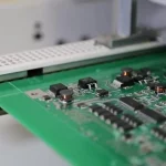
<img src="https://www.gopcba.com/wp-content/uploads/2025/05/未标题-5.webp" alt="solder paste printing stage on an SMT line” />
Placement Accuracy
Placement is the most visible stage and the easiest to measure, which is why it receives the most attention. Accuracy requirements scale with the smallest feature on the board: chip components tolerate a positional error an order of magnitude larger than fine-pitch packages and area array devices do.
What drives the achieved accuracy: the vision system and how well it is calibrated, nozzle selection for each component size and shape, the pick height at which the part is taken from the tape or tray, the placement force applied during placement, and the speed at which the machine runs. Speed is the parameter that trades directly against accuracy, and a programme run near the machine’s limit has very little margin left for anything else.
Placement force deserves particular attention on small packages. Excessive force displaces the component in the paste, which moves the part and, in the case of a two-terminal chip, can tilt it far enough that it stands up during reflow.

The Reflow Profile
Reflow forms the joint by melting the alloy and allowing it to wet both the component termination and the pad, then cooling it into a solid connection with a thin intermetallic layer at each interface.
The profile is described in four zones, and each one has a purpose. The preheat zone raises the board from room temperature to roughly 150 °C at a modest rate, so the flux begins to activate and volatile solvents are driven off without spattering. The soak zone holds the assembly between roughly 150 °C and 180 °C, letting the whole board equalise in temperature so that small and large thermal masses reach the liquidus together. The reflow zone takes the alloy above its melting point to a peak, and the time spent above liquidus controls how much intermetallic grows. The cooling zone brings the joint down at a controlled rate, because cooling too quickly produces a brittle, coarse grain structure and cooling too slowly allows the joint to remain in a weakened state.
The profile is not transferable between products. Board thickness, copper area, component mass and the density of the assembly all change how the heat arrives, and a profile that suits one product may leave a heavy thermal mass under the liquidus while a small one nearby is well past it.
Defects and What They Indicate
Tombstoning is the classic two-terminal failure: one end of a chip component lifts and stands against the pad after reflow. It comes from a heat imbalance between the two pads, which may originate from unequal pad or trace geometry, from a component placed off centre, from a difference in paste volume, or from the two ends of the part reaching the liquidus at different moments. The correction is usually geometric before it is thermal.
Bridging is paste or solder joining two adjacent conductors. Excess paste, an oversized aperture, excessive print pressure, too much placement force and pitches that leave no room for the paste to collapse all contribute.
A cold joint or a partially reflowed joint looks connected and is not: the alloy has not fully melted, or the surfaces were not clean enough to wet. Insufficient peak temperature, a profile with too little time above liquidus, oxidised pads and insufficient flux activity are the usual causes.
Solder balls are small spheres left on the board surface. They come from paste spattered during a fast preheat, from paste extruded beyond the pad under excessive placement force, from moisture absorbed in components that flashes out at temperature, and from poor stencil underside cleanliness between prints.
Inspection and What It Can See
Optical inspection after reflow compares the appearance of each joint against a reference and finds missing components, misalignment, rotation, the polarity errors, and visible joint defects such as bridges, insufficient fillets and loose balls. It cannot judge the internal quality of a joint, and it cannot see underneath an area array package at all.
That gap is filled by X-ray, which shows the projected image of the joints beneath the package and reveals voids, bridges and open connections that optics cannot reach. Where the design includes area array devices, X-ray is not an optional inspection stage; it is the only inspection stage that addresses those joints.
Earlier in the line, paste inspection after printing measures deposited volume before any component is placed. It is the one inspection whose findings can be corrected by simply cleaning the stencil and printing again, which makes it the cheapest defect detection in the process.
Holding the Process Between Batches
Parameters drift. Paste ages, stencils stretch, nozzles wear, heaters lose efficiency, and vision systems accumulate calibration offset. The controls that keep a process comparable across batches are the unglamorous ones: printing parameters recorded and verified at the start of each run, first article inspection before the batch continues, periodic profile measurement with a profiler rather than reliance on the machine’s displayed setpoints, and inspection criteria that stay fixed rather than being adjusted to accept what the line is producing.
Assemblies that combine this process with board fabrication and test are handled under one sequence in our overview of SMT PCB assembly, with verification covered under PCBA testing and the record-keeping side under quality management.
FAQ
Which stage causes most defects? Printing. The deposit it leaves determines whether the joint can form, and errors introduced there are only visible after reflow, when the board has already been built on.
Why does a component stand up during reflow? Usually unequal heating or unequal paste volume between its two pads, or a placement offset that leaves the component balanced on one end.
Is optical inspection enough? For visible joints, generally yes. For joints beneath area array packages it sees nothing, so X-ray is required wherever those packages are used.