PCB Design Preparation: Goals, Libraries and Standards
Layouts that run late rarely fail because the routing was too difficult. They fail because the work started before anyone agreed what the board was for, or before the footprint of a critical part had been checked against its datasheet. PCB design preparation is the unglamorous half of the project, and it is the half that determines how much of the schedule survives.
Define What the Board Must Do
The first task is to fix the design goals and the application context, because they set almost every downstream choice.
A board for consumer electronics, an industrial controller and a communications unit differ in performance requirements, functional expectations, operating environment and cost budget, even when the circuits look similar on paper. A consumer product may accept a narrower temperature range and a tighter cost target, while an industrial unit will be asked to run hotter, longer and with more protection.
Writing those goals down does more than document intent. It tells the designer which requirements are fixed and which are negotiable, which is the information needed to make the hundreds of small trade-offs that layout involves without stopping to ask each time. Layer count, material grade, connector choice and test coverage all follow from this statement.
Collect the Design Data
Design work needs a complete input set before it can begin efficiently.
The schematic is the primary document: it defines the devices and the electrical connections that the board must realise. The bill of materials turns those devices into specific parts with package information, and it is the basis for choosing footprints. Alongside them go the technical specifications and the standards that apply to the product — electrical requirements, environmental conditions, mechanical constraints, and the acceptance criteria against which the finished board will be judged.
Incomplete inputs are the usual cause of a design that has to be restarted. If the mechanical drawing arrives after placement is finished, the placement is redone. If the specification for impedance arrives after stackup selection, the stackup is redone. Gathering the set first is cheaper than discovering it piece by piece.
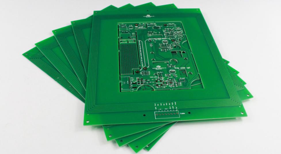
<img src="https://www.gopcba.com/wp-content/uploads/2026/08/PCB-Fabrication-Process.jpg.webp" alt="PCB design preparation with schematics and component library” />
Choose and Learn the Tools
The design software is selected before the work starts, and the choice matters less than the familiarity with it. A commercial EDA suite provides schematic capture, layout, design rule checking and output generation in one environment; the differences between packages are far smaller than the difference between an engineer who knows their tool and one who does not.
What should be settled in advance is the tooling convention: which library the project will use, which design rule set will be applied, and how outputs will be produced and named. Teams that agree this at the start avoid rework at the end, when a design rule set that does not match the manufacturer’s capability turns into a batch of false errors and a delayed release.
Build the Component Library First
The component library is where preparation most often gets skipped, and where the cost of skipping it is highest.
The library must contain both the schematic symbol and the PCB footprint for every device on the board, and the two must agree. For standard parts, an existing library can be used, provided it is verified rather than trusted. For unusual or newly released devices, both symbol and footprint usually have to be drawn from the datasheet.
Drawing a footprint is a mechanical task with mechanical consequences. Pad size, pitch, pad shape and courtyard must follow the actual package dimensions and pin layout, and they must account for the manufacturers’ tolerances and for the assembly process, not merely the nominal drawing in the datasheet. A footprint that is slightly too small produces solder joints that look marginal and fail inspection; one that is slightly too large produces components that shift during reflow. Either way, the error is invisible until hardware exists, which is why library parts are checked by a second person rather than accepted on completion.
Plan the Dimensions and the Structure
Board size and shape come from the product, not from convenience: the outline has to fit the enclosure, and mounting holes, connector positions and keep-outs are fixed by the mechanical design.
The layer structure is then planned against the electrical requirements. Complex boards will need a multilayer construction, and the stackup has to assign signal, power and ground layers deliberately so that every high-speed net has a reference and every plane is continuous where it matters. Deciding this before layout starts avoids the situation where the routing is nearly complete and the stackup turns out not to support the interfaces on the board. That assignment process is set out in this discussion of multilayer layer assignment.

Know the Standards You Are Designing To
Preparation also means reading the applicable industry standards before, not after, the routing is finished. IPC standards, for example, cover component placement, routing rules, electrical clearance and creepage distance, pad sizes and via design. They exist because the properties they specify determine whether the board can be manufactured repeatably and whether it will still be safe at the end of its life.
Clearance and creepage are the two that most often catch a first-time designer. They are not the same requirement: clearance is about the air gap that withstands a voltage, creepage is about the distance along the surface, and the surface path is affected by contamination and humidity in service. A board that meets one and not the other will pass initial testing and fail in the field.
Aligning these requirements with the actual capability of the fabricator is part of the same exercise. Standards define what is acceptable in general; a specific shop defines what is achievable on their lines, and the design rules used should be the tighter of the two. Where the two are far apart, the gap usually shows up as cost or yield, which is one of the things worth assessing before committing, as described in these notes on evaluating a PCB design company.
Why Preparation Pays for Itself
The work described above is short compared with the layout itself, and it prevents the three most expensive categories of rework: a placement redone because the mechanical constraints arrived late, a stackup redone because the electrical requirements were not known, and a prototype rebuilt because a footprint did not match the part. The information pack that results from this preparation is the same one a layout team needs to begin work at all, and it is set out item by item in this summary of PCB design inputs and steps.
FAQ
Can preparation be shortened for a simple board? It can be compressed, but not skipped. A two-layer control board still needs a verified footprint library, a defined outline and a rule set; what changes is the depth of the stackup and simulation work.
Whose library should be used, ours or the designer’s? Either can work, provided one library is authoritative for the project. Mixing two libraries that define the same part differently is how a board ends up with two incompatible footprints for one device.
Why check creepage as well as clearance? Because they fail differently. Clearance protects against breakdown through air at a given voltage; creepage protects against tracking across a contaminated surface over time. A design that satisfies only the first can appear sound and still degrade in service.