PCB Outline Efficiency and Mechanical Fit
The outline is the first thing fixed in a design and the last thing anyone wants to change. It comes from the mechanical engineer, it has to fit an enclosure, and it determines how the board is handled through every process. Because it is treated as given rather than as a design variable, the opportunities it offers are often missed, and the penalties it imposes are often accepted without question.
The Envelope and the Board
The board outline comes from the enclosure, but the two are not the same shape. The enclosure provides a cavity, and the board occupies part of it, leaving space for connectors, cable routing, battery, display and the mechanical features that hold everything in place. The board must also clear the ribs, bosses and screw pillars that stiffen the housing, and it must allow the assembly to be inserted without the connectors fouling the opening.
Getting this right is an iterative process rather than a one-way handover. The mechanical engineer produces the cavity, the electrical engineer places the components, and the component heights and connector positions come back to the mechanical engineer, who adjusts the housing. The mechanical fit that results is a compromise, and the earlier the loop is closed the fewer iterations it needs. The design constraints that mounting features impose on the layout are described in this article on board outline and mounting design.

Keepout Regions and Their Enforcement
A keepout region is an area where components and copper are not allowed, for a mechanical rather than an electrical reason. Typical keepouts cover a screw boss on the housing lid, the travel path of a connector latch, the area swept by a hinged part, and the clearance needed for the tool that tightens a fastener.
The effective way to handle keepouts is to define them as regions in the layout tool rather than as notes on a drawing. A region is enforced automatically, so a component placed there will generate an error, while a note is only as reliable as the memory of the person reading it. The same applies to height restrictions, which should be expressed as a maximum component height per area rather than as a general instruction.
Panelization and Outline Shape
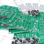
The board is not manufactured alone. It is placed on a panel with other boards and with the tooling features the process requires, and the outline shape determines how efficiently that panel can be arranged. A rectangular board of modest size can be arranged in an array with minimal waste; an irregular outline leaves gaps between boards that cannot be used.
The gain from reconsidering the outline is sometimes substantial. A small change to a corner radius, the removal of a decorative tab or the relocation of an internal cutout can allow a tighter array, and the saving applies to every unit produced. Panelization also determines where the board is supported during assembly, which in turn affects whether the paste printing and placement are consistent. The features that a panel requires are described in this discussion of PCB slot and edge routing.
Edge Clearance and Routing
The board edge is a manufacturing feature as well as a boundary. Copper must be kept back from the profile so that the routing operation does not expose or damage it, and the amount of clearance depends on the fabricator and on the finish. Components must be kept further back still, because a part placed against the edge can be struck by a conveyor, a fixture or a depanelling tool.
The routed edge also carries a radius at every internal corner, because the cutter has a diameter. A design that asks for a square internal corner cannot be produced as drawn, and the fabricator will either modify it or return the design. Specifying the radius in the design avoids that conversation and ensures the mechanical fit is calculated against the shape that will actually be produced.
Outline Efficiency in Practice
Efficiency comes from aligning three things: the mechanical requirement, the fabrication process and the assembly process. The mechanical requirement fixes the outline within a tolerance. The fabrication process prefers regular shapes, straight edges and features aligned in one direction, because those allow a continuous tool path and a tighter panel array. The assembly process prefers a shape that can be supported on a flat fixture and held without flexing.
Where a design can satisfy all three, the cost is lower and the yield is higher. The changes needed are usually small: squaring a chamfer, moving a cutout a few millimetres, or accepting a slightly different connector that allows the board to be rectangular. Each of those decisions is cheapest at the concept stage and progressively more expensive afterwards, which is why the outline deserves to be reviewed by the electrical engineer rather than accepted without comment.
A Checklist for the Outline
Before the outline is frozen, confirm that it matches the current mechanical drawing, that every keepout is expressed as an enforced region, that internal corners carry a radius at least half the router diameter, that copper and components are kept clear of the profile by the required distance, and that the shape allows an efficient panel array. Those five checks take an hour and they determine a large part of the manufacturing cost and the assembly yield of the product.
Outline Changes and Their Consequences
An outline change late in a project propagates further than it appears to. Moving an edge by a few millimetres changes the position of every component that was placed relative to that edge, alters the length of the traces that reach the connectors along it, and may invalidate a panel array that has already been agreed. The mechanical change itself may be trivial while the electrical consequences are not, which is why the outline should be frozen before routing rather than during it. Where a change is unavoidable, the review described in this article on board outline and mounting design should be repeated for the affected regions rather than for the whole board.
Where the board edge clearance is tight, the enclosure and the assembly method should be reviewed together rather than separately, because the clearance that the fabrication process needs is not always the clearance the assembly process needs. A component that satisfies the fabrication limit may still be vulnerable to a depanelling tool, and the difference between the two requirements is worth establishing before the outline is finalised.
FAQ
Can the electrical engineer change the board outline? It is a mechanical requirement, so the change belongs to the mechanical engineer, but the electrical engineer should review it for manufacturability and report anything that will raise the cost or complicate the panelization. The conversation is cheapest at the concept stage.
How much clearance is needed between copper and the board edge? Enough that the routing operation does not expose or damage the copper, and the figure should come from the fabricator for the specific finish and construction. Components need more clearance than copper, since they must survive handling and depanelling.
Why does the outline shape affect cost? Because the board is built as part of a panel. A regular outline allows a tight array with little waste, while an irregular one leaves gaps that cannot be used, and the waste is paid for in every unit produced.