Board Outline and Mounting Design for PCB Layout
Layout is usually described as an electrical discipline, but a large part of it is mechanical. The board has to fit inside an enclosure, be held in place, accept connectors that align with openings, and survive the assembly process. Every one of those requirements constrains where copper may go, and the constraints are fixed long before the routing begins. Ignoring them until the layout is nearly complete is the most common reason a design has to be rebuilt from scratch.
Who Owns the Board Outline
The board outline is not a layout decision. It is a mechanical requirement produced by the industrial designer and the mechanical engineer, expressed as a drawing with dimensions, tolerances and mounting features, and it becomes an input to the electrical layout along with the schematic and the stackup. The two sets of documents feed each other: the mechanical drawing fixes the outline, and the layout returns the component heights and the connector positions that the enclosure must accommodate.
The process is iterative. Early in a project the outline is provisional and the layout explores what fits; later the outline is frozen and the layout conforms to it. Version control matters here, because a layout built against an obsolete outline will be wrong in ways that no electrical check can detect.
Corner Radii, Slots and Panel Handling
Sharp corners on a board outline are a manufacturing problem. The routing tool that cuts the profile leaves a stress concentration at an internal corner, and boards break at that point during depanelling or handling. Every internal corner should carry a radius large enough for the router bit used by the fabricator, and the external corners should be rounded as well to avoid snagging.
Slots and cutouts need the same treatment plus an additional consideration: the router needs clearance to approach the feature, so a slot narrower than the tool diameter cannot be machined. Long thin sections of board are also mechanically fragile and should be avoided where possible, or supported by panel tabs during assembly.
Mounting Holes and Keepout Zones
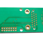
A mounting hole exists to be loaded. A screw or standoff applies compressive force, and the copper and laminate immediately around the hole experience that force along with whatever mechanical stress the assembly introduces. The result is a set of keepout zones around each mounting hole that are larger than the hole itself.
As a working rule, no copper and no component should sit within about 1 mm of the hole edge on the top and bottom copper layers, and the zone should be extended where the hole is a plated or grounded one. Where the mounting point is also used as a chassis ground connection, the copper ring around it should be sized for the current and stitched to the internal ground planes with multiple vias, and the surrounding region should be free of signal traces so that the screw head does not create a short.
Keepouts also apply around the board edge. Copper should generally be kept 0.2 mm to 0.5 mm inside the profile, depending on the fabricator”s capability, so that the plating and routing operations do not expose or damage the copper. Components should be kept further back still, and the rules for how far copper should sit from a pad or a hole are set out in this article on via to trace clearance.
Connector Placement and Alignment
Connectors define the electrical interface and the mechanical interface at the same time. Their position along the board edge determines whether a cable can reach them and whether the mating half aligns with the enclosure opening. Connector placement should therefore be fixed early, in consultation with the mechanical drawing, and treated as a constraint on the layout rather than a convenience for the router.
Two rules follow from mechanical stress. Traces should escape from the centre of the connector pad and continue outward in the direction the pad is oriented, because an angled escape creates a stress concentration that tears when the connector is mated and unmated. And the connector body requires clearance on all sides for the mating action, the latch or screw, and the tool used to assemble it. The escape geometry itself is described in more detail in this discussion of escape routing and pad fanout.
Component Height and Keepout Volumes
Electrical keepouts are flat; mechanical keepouts have height. A tall electrolytic capacitor in the wrong place can foul a boss on the enclosure lid, and a component placed under a connector body may be impossible to solder or inspect. The layout should therefore carry a height map for the critical areas: the volume reserved for the enclosure wall, the volume reserved for the lid, and the volume needed for the mating connector.
These constraints are best expressed as keepout regions in the layout tool rather than as notes on a drawing, because the tool will enforce them. A height-limited area marked on the layout prevents the placement of a part that would later have to be moved.
Test Points, Fiducials and Panelization
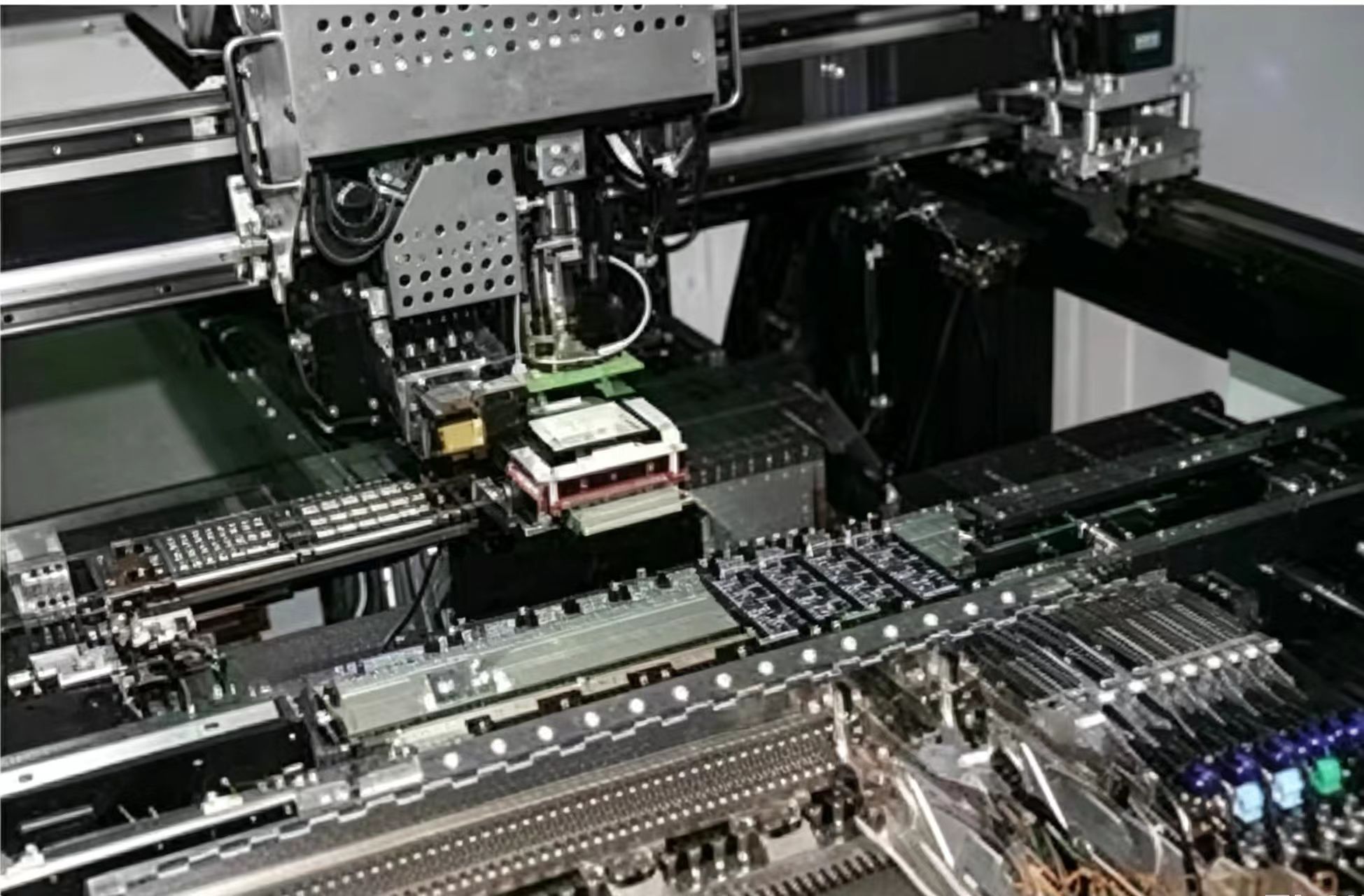
Assembly tooling needs features that have nothing to do with the circuit. Fiducials are copper marks with a clear area around them that allow the placement machine to locate the panel; they should be placed in three corners of the panel and on each individual board where the panel is large. Test points for in-circuit test need to be accessible from one side and surrounded by clearance for the probe.
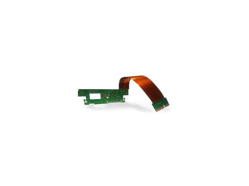
Panelization is the arrangement of boards within a manufacturing panel, and it interacts with the outline. Tabs and breakaway rails add material that must be removed after assembly, and the position of the tabs determines which edges are cut and which are routed. Where a design includes edge connectors, the tooling strips and the direction of the gold fingers constrain the layout of the panel, so the decision has to be made before the outline is finalised. Getting the flatness and dimensional requirements right is also a fabrication concern, since the checks a fabricator applies to layer stackup and thickness interact with the panel construction.
Reviewing the Mechanical Constraints
Before the layout is released, the engineer should confirm four things: that the outline matches the current mechanical drawing, that every mounting hole has its keepout honoured on all layers, that every connector has the clearance its mating action requires, and that the panel construction has been agreed. These checks take minutes and they prevent the kind of error that costs a project a month.
FAQ
How much clearance should I leave around a mounting hole? As a starting point, keep all copper and components at least 1 mm clear of the hole edge on the outer layers, and extend the zone where the hole is plated or used as a ground connection. Where a screw head will sit, the keepout must cover the full diameter of the head.
Why do internal corners on a board outline need a radius? Because the router leaves a sharp notch that concentrates mechanical stress, and the board will crack there during depanelling or handling. The radius must be at least as large as the router bit the fabricator uses for the profile.
Who decides the board outline? The mechanical engineer produces it as a drawing, and it becomes an input to the layout along with the schematic. The layout then returns component heights and connector positions so the enclosure can be adjusted, which is why the two processes are iterative rather than sequential.