Parallel Bus and Serial Bus Routing Rules for PCB Layout
Almost every high-speed interface on a modern board is either a parallel bus or a serial bus, and the two families fail for different reasons. A parallel bus fails when one lane arrives at the wrong time; a serial bus fails when the signal that arrives is too small or too distorted to be recovered. Knowing which family a net belongs to determines what the layout has to protect, and it is the first question worth asking before routing begins.
What a Bus Is and Why the Distinction Matters
A bus is a shared physical path used by two or more devices to exchange information, and it is built from a group of related signal lines that share a common protocol and a common timing reference. The classification into parallel and serial describes how the payload is spread across those lines at any instant. In a parallel bus, several bits travel at the same time and the group is meaningless unless every line arrives together. In a serial bus, bits travel one after another on a single lane or a pair of lanes, and each bit is interpreted independently in time. The consequence for layout is that a parallel bus is dominated by timing, while a serial bus is dominated by signal amplitude and frequency-dependent loss, and the two therefore respond to different layout mistakes.
Parallel Bus Behaviour
A memory data bus is the classic example: a group of data lines with a strobe and a mask, transferring a word at a time. Because the receiving device samples all of the lines on the same edge, the validity of the whole transfer depends on the worst lane. If one line is significantly longer than the others, the data eye closes for the entire group rather than for that line alone, and the transfer simply fails and is retried. This is why a parallel bus is routed as a group, why the lines within a byte lane are adjusted to match each other, and why serpentine routing is used to add length where a line would otherwise be short.
<img src="https://www.gopcba.com/wp-content/uploads/2023/05/pierre-chatel-innocenti-Lk-nu_hX6ms-unsplash.jpg" alt="parallel bus traces routed with length matching on a PCB” />
Serial Bus Behaviour
A serial bus carries one bit at a time, so a single distorted bit does not invalidate its neighbours the way a parallel lane does. The difficulty moves into the channel: the link must deliver enough amplitude and enough bandwidth for the receiver to recover each bit, and the channel’s loss, reflections and crosstalk decide whether that is possible. At multi-gigabit rates the trace behaves as a transmission line with a loss that grows with frequency, and the features that matter become the impedance profile, the number of layer changes and the quality of the vias along the path rather than the relative length of neighbouring lines.
Parallel Bus Routing Rules
Route the bus on inner layers wherever possible and open up the spacing to unrelated nets. Single-ended lines are normally designed for 50 ohms and differential pairs for 100 ohms, unless the interface specification says otherwise. Lines within a lane should be kept close to equal length and should follow the timing relationship with the strobe or clock that the timing analysis defines. The group should reference a continuous plane, and any net with a rise time below about 1 ns must have a complete reference plane with no crossing of a plane split. Where a serpentine is used to add length, the spacing between adjacent sections should be at least three times the trace width to keep the added coupling small; the technique is described in this article on serpentine routing and length matching. Lower-order address lines, which are less sensitive to timing, can follow the clock routing rules where the bus topology allows it.
Serial Bus Routing Rules
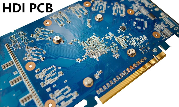
Above roughly 100 Mbps the loss of the channel starts to set the limits, so trace width and trace length should be chosen together rather than independently. A working minimum for the line width is 5 mil, and the route should be as short as the topology permits. Layer changes should be avoided except where an escape requires them, because each via adds a discontinuity and a stub. At 3.125 Gbps and above, the anti-pad geometry of the vias involved should be optimized to reduce the impedance discontinuity, and ground vias should be placed beside the signal via. A blind or back-drilled via that leaves the shortest stub is preferable, and when stub length must be traded between two ends, the shorter stub belongs to the transmitter side. Signals travelling in opposite directions should not be routed on top of each other, and the edge of a high-speed route should stay at least three trace widths away from the edge of any plane split.
Choosing Layers and Controlling Impedance
Both families benefit from being routed against a solid reference plane, but the reasons differ. For a parallel bus the plane is the return path that keeps the lines’ timing consistent; for a serial bus it is part of the transmission line that sets the impedance. Impedance control is therefore a stackup decision before it is a routing decision, and the trace geometry must be derived from the finished dielectric thickness and copper weight rather than assumed. Where a bus must change reference planes, a stitching capacitor or a ground via placed near the transition keeps the return path continuous, and the general approach to bus routing is set out in this article on high-frequency traces and data bus routing.
Escape, Fanout and Layer Transitions
Most of the difficulty in a busy design sits at the escape from a fine-pitch package. Fanout vias consume routing channels, and a bus that cannot escape in order will end up with crossed pairs and unnecessary layer changes. Planning the escape before the general routing, and reserving the via pattern for each lane, keeps the group parallel through the transition. The rules that govern channel width, via-to-trace clearance and escape patterns are collected in this article on escape routing and fanout rules.
Verifying Before Release
Before the design is released, both families should be checked for the same small set of items: the impedance target against the actual stackup, the reference plane under each fast net, the length spread within each parallel lane, the number of layer changes on each serial lane, and the distance between any plane split and a signal edge. These five checks take about an hour and cover most of the reasons a first prototype fails to link up at all.
FAQ
Why must a parallel bus be length matched if the lines are all the same length on the schematic? The schematic carries no length information. Physical length differences appear only in layout, and a single long lane delays the whole transfer.
Do serial buses need length matching? Within a differential pair, yes, because the two conductors must stay in phase. Between pairs, the skew tolerance is usually loose enough that matching is not the limiting factor.
When is via stub control necessary? When the data rate reaches the multi-gigabit range and the stub is long relative to the rise time. At that point blind vias or back drilling are used to shorten or remove the stub.