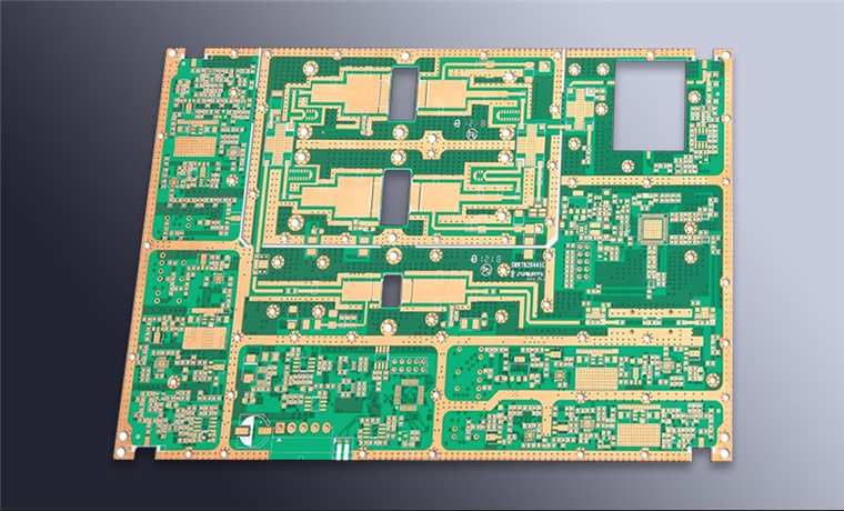
Where PCB Prototyping Goes Wrong and Why
A prototype exists to answer questions, and it fails at that job when the questions were poorly chosen. Most prototyping problems are not manufacturing defects. They are decisions taken before the order was placed, in the quantity ordered, the footprints used, the testing planned and the electrical assumptions made. Each is predictable, and each is cheap to address in advance.
Getting the Quantity Right
The number of boards to build should follow from the number of things being tested. A single unit tests function but leaves nothing to sacrifice for destructive analysis or for a rework experiment, and if the first board is damaged the schedule loses a full cycle.
Ordering enough boards to cover the tests, plus spares for the faults that will appear, is usually cheaper than a second run. That is especially true when the design carries expensive parts, because the fixed cost of tooling and setup is paid again on the repeat order. The prototype cost structure is dominated by setup rather than by material on small quantities.
Footprint Errors
An incorrect component footprint is the most common reason a first prototype cannot be assembled. The schematic is electrically correct and the netlist passes, but the physical pad pattern does not match the part that arrives.
Footprint libraries are a frequent source of this. A library may hold a package with the right name but the wrong pad dimensions, or a datasheet may specify a pad pattern that differs from the recommended land pattern for the assembly process. Verifying the footprint against the actual part, and printing the layout at one to one scale to compare it with a sample, catches the error before fabrication. Our prototyping workflow notes describe where that check sits in the sequence.
Skipping Electrical Test
A prototype that is not tested electrically at bare board stage carries an unknown into the assembly step. A short between two nets or an open on an inner layer will waste the components that are placed onto it.
Bare board electrical test is inexpensive relative to the value of the parts and the assembly time, and it converts a board of unknown status into a board with a defined starting condition. Where a fault is found later, the assembled board can be scrapped with the certainty that the source was the assembly, not the bare board. Test methods and their limits are set out in our article on PCB electrical test coverage.
Signal Integrity Assumptions
Prototypes often expose problems that were invisible on paper. A bus that simulated cleanly may show ringing on the bench because the return path was interrupted by a plane split, or because a driver is faster than the model assumed.
The remedy is to bring up the board with a measurement plan rather than a checklist. Decide in advance which nets to probe, what waveform is expected and what would count as a failure, so that the board can be measured while it is on the bench rather than after the design has been changed. Our eye diagram and the spacing rules in our PCB layout tips article notes cover the measurements that make this objective.
Layout Choices That Cost a Rebuild
Some layout decisions only reveal themselves after assembly. A connector placed where it interferes with the enclosure, a test point covered by a tall component, or a programming header that cannot be reached with the board installed are all mechanical conflicts rather than electrical ones.
Checking the prototype against the enclosure and against the assembly fixtures, before the order rather than after, removes an entire class of rework. Mocking up the board outline in card and fitting the real connectors into it takes minutes and finds these problems reliably.
Documentation and Version Control
A prototype is a physical document of a specific revision, and it is worthless if that revision cannot be identified. Silkscreen markings, a version field in the firmware and a record of which changes were made after assembly keep the board traceable.
The change list matters most. A prototype that was hand modified during bring-up must be documented, or the next revision will be built with an error that was already corrected on the bench, and the correction will be lost. A design release checklist gives the release its structure.
Planning the Bring-Up Before the Order
Prototype cost is easier to justify when the plan is written before the boards are ordered. List what will be measured, which nets will be probed, which firmware functions will be exercised and what result counts as a pass. A board that arrives without that plan tends to be tested informally, and informal testing finds the obvious faults while missing the marginal ones.
Decide as well who will assemble and rework the board. Hand assembly of a fine pitch prototype demands different tooling and skill from a production run, and knowing this in advance avoids a scramble when the first unit is built.
Bring-Up Records
Keep a written record during bring-up. Which changes were made, which components were swapped, which measurements were taken and at what supply voltage. That record is what turns a working board into a repeatable design, and it is what allows the second revision to be built without rediscovering the same problems.
The record also protects the schedule. When a fault appears a week later, the note that describes the same symptom and the fix that resolved it saves a day of investigation, and it prevents a known issue from being carried into the next revision unnoticed.
Prototype Cost and Where It Goes
Prototype cost is dominated by fixed items rather than by material. Tooling, stencil, first article inspection and setup are paid once regardless of quantity, so the cost per board falls quickly as the order size rises.
That is the argument for ordering the boards the test plan actually needs in one purchase rather than in successive small orders. Two small orders pay the fixed cost twice, and the second order arrives later than the schedule can usually afford. The economics are the same ones that shape our prototype BOM planning advice.
Component Footprint Verification in Practice
A component footprint can be verified in a few minutes before the order is released. Print the layout of the critical parts at one to one scale, place the real components on the print and compare the pad edges against the leads.
Doing this for connectors, fine pitch packages and any part that was added late in the design catches the majority of footprint errors. It also reveals land patterns that are technically correct but leave insufficient solder fillet for inspection, which is a manufacturability problem rather than a connectivity one.
FAQ
How many prototype boards should be ordered? Enough to cover the planned tests plus a spare or two for the faults that will appear, which is usually cheaper than a repeat run with its own setup cost.
Can footprint errors be caught before fabrication? Most of them can. Comparing the land pattern against the datasheet and the real component, and printing the layout at full scale, catches the majority.
Is signal integrity testing necessary on a slow design? It is necessary on any design with fast edges, even if the clock is slow. If a net has a rise time short enough to make its traces electrically long, it deserves measurement.