IoT PCB Design: Standards, Low Power and RF Integration
An IoT product combines four things that are individually difficult and together are unforgiving: a radio, a battery, sensors with small analogue signals, and a fast digital core, all inside a package the size of a coin. An IoT PCB design has to satisfy all of them at once, and the constraints that come from the standards and from the power budget tend to decide the layout before any routing is considered.
Start With the Standards
If the device will be sold, it has to meet the standards that apply to it, and those standards impose layout requirements rather than merely test requirements. IPC standards define what the board itself must be able to withstand. Safety standards define clearance and creepage. Radio regulations define the bands and the permitted emissions, and they usually constrain the radio section rather than the whole board.
Working to the standards from the start costs nothing. Discovering them after the layout is finished costs a redesign, because the changes they demand are geometric: more clearance here, a different stackup there, an antenna with a different keepout.
Low Power Design and Sleep Modes
A mains-powered device can ignore idle current; a battery device cannot. Most IoT devices spend the overwhelming majority of their life asleep and wake briefly to measure, transmit and return to sleep. The design has to make that pattern work, which means that every block must be able to be turned off completely, and that the leakage of the turned-off blocks must be small compared with the active current of the rest.
That requirement reaches into the layout. Pull-up resistors that stay connected waste current continuously. A regulator with a high quiescent current wastes more than the load. A voltage divider used for measurement should be switched in only when the measurement is taken.
Block by Block Power Budgets
The practical method is to divide the board into functional blocks and assign an energy budget to each: the radio, the processor, the memory, the sensor front end, the power conversion. Then check each block against its budget, and check the sum against the battery.
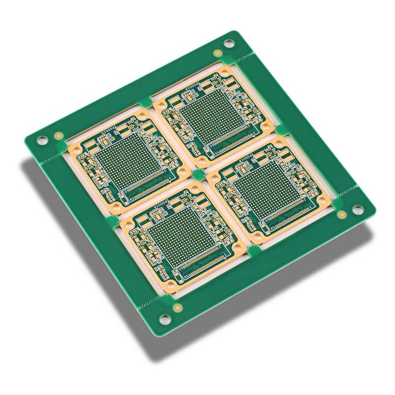
Where a block exceeds its budget, the answer is usually a different component rather than a different layout, and the component supplier can often recommend a lower-power alternative with the same function. Allocating the budget before the schematic is fixed is what makes this possible.
Memory Choice and Its Effect on Current
Memory selection is a power decision as much as a capacity decision. Each type has a different trade between density, cost, standby current and access latency, and mixing types is normal in a device that needs both working memory and storage. The important point for the layout is that the high-current memory device should be placed close to its supply and its decoupling, and that its bus should be short.
Working With an RF module
Most IoT designs should not integrate a radio from discrete components. A pre-certified module has already passed the regulatory testing, which removes an entire category of risk from the project, and it usually occupies less area than an equivalent discrete design.
Choosing an RF module also fixes several layout parameters in advance: the supply voltage and current, the required ground plane size, the keepout around the antenna and sometimes the position of the module on the board. Those parameters become constraints on everything else, which is another reason to choose the radio early rather than late.
What the module does not remove is the layout requirement. The module needs a defined ground plane beneath and around it, its antenna needs a keepout that the rest of the layout respects, and its supply needs to be quiet. A certified module placed badly will still fail its emissions limits. EMI suppression design principles covers the measures that keep a radio inside its limits.
Antenna Keepout and Ground
Antenna placement is the most constrained decision in the whole layout. The keepout must be free of copper, components, battery and metal, in three dimensions, and the feed line must be a controlled-impedance trace with a solid reference. If the antenna is a chip type, it also needs a specified ground plane size to work as designed, which means the board dimensions are part of the antenna design.
Placing the antenna at one end of the board and the switching supplies at the other is the standard arrangement, and it should be decided before anything else is fixed.
Mixed-Signal Sections
Sensor interfaces are analogue, and their signals are often small. The separation rules are the familiar ones: keep the analogue front end away from the digital core and the radio, keep the high-impedance nodes short, and give the analogue section a local reference that returns to the main plane at a point you control rather than at a point chosen by the router.
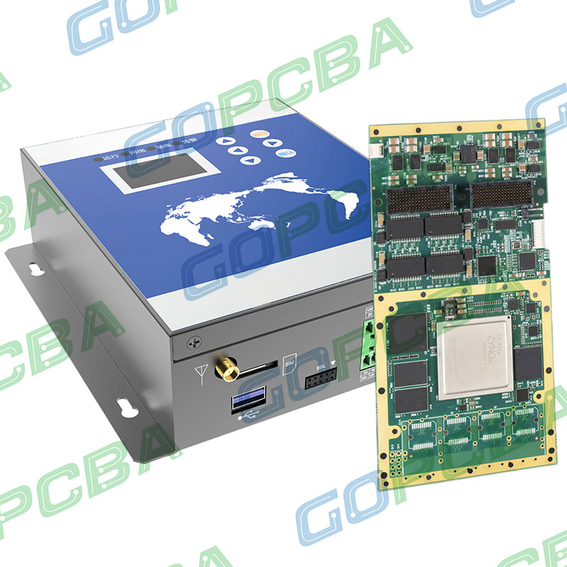
A single continuous ground plane with managed return currents is more reliable than splitting the ground into named regions, and it is easier to review. Mixed-signal PCB design guidelines sets out the arrangement in detail.
High-Speed Signals in a Small Space
The digital side of an IoT device may include a high-speed interface to memory or to a display, and those signals need controlled impedance and length matching just as they would on a larger board. In a small enclosure the temptation is to accept whatever routing fits, which is how a device ends up with an intermittent memory error that only appears at temperature extremes.
Decide the stackup early, keep the impedance-critical nets on a layer with a solid reference, and do not let the antenna keepout push the high-speed routing into a region where the reference is broken. AIoT processor core board design covers the arrangement of a processor, memory and radio on a compact board.
Prototyping and Iteration
Mixed Signal Design Discipline
Good mixed signal design on an IoT board is mostly about placement and return paths, not about exotic components. Put the analogue front end at the end of the board furthest from the radio and the switching regulators, keep its traces short and its impedance low, and give it a local ground pour that connects to the main plane at a single point you have chosen deliberately.
Where a converter sits between the analogue and digital sections, place it at the boundary so that its digital pins face the digital area and its analogue pins face the analogue area. Then leave the boundary alone: a trace that crosses it carries the switching noise of one domain into the other, and no amount of decoupling will undo that. Recording the boundary on the layout, as a line on a mechanical layer, makes it obvious during review when something has crossed it.
IoT products usually go through more iterations than their complexity suggests, because the radio performance and the current consumption in each sleep mode are not fully predictable from a schematic. Building the first prototype on the intended stackup, with the intended antenna and enough test access to measure the supply current of each block separately, makes those iterations informative rather than merely hopeful.
FAQ
Should the radio be a module or a discrete design? A module unless there is a strong reason otherwise. It transfers the certification risk to the module vendor and usually reduces the board area as well.
How much current can a coin cell supply? Very little continuously, and only tens of milliamps in short pulses. That limit is what drives the block-level energy budget, and it is worth checking against the radio’s transmit current before the design is committed.
Does a certified module remove the need for EMC testing? No. The module certification covers the module in its reference configuration. The assembled product still has to meet the emissions requirements as a whole, and the layout determines whether it does.