



Mixed Signal PCB Design Guidelines
Boards that contain both analog and digital circuits are the most common source of difficult layout problems, because the two halves of the design want opposite things. Analog circuitry measures small continuous signals and needs a quiet, stable reference. Digital circuitry switches state abruptly, draws current in spikes and produces broadband noise. Put them on the same piece of copper and the digital noise appears directly in the analog measurement.
What Makes the Problem Hard
A mixed signal board combines circuits that process continuously varying signals, such as sensor conditioning chains and reference buffers, with circuits that process discrete states, such as microcontrollers and digital signal processors. The analog circuits care about microvolts and are disturbed by anything that changes the voltage of their reference. The digital circuits operate at frequencies whose harmonics extend far beyond the clock rate and inject current into the ground network on every transition.
Both circuits are referenced to the same ground network, and the ground network has resistance and inductance. That is the whole problem. Any current flowing through the ground produces a voltage, and every circuit connected to that point sees the voltage as part of its signal.
Partitioning the Board
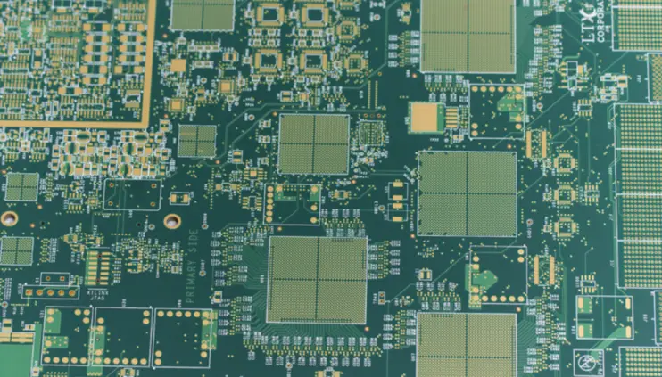
The first and most effective measure is physical separation. The analog components, their traces and their ground should occupy one region of the board, and the digital components another, with the interface between them concentrated in as few places as possible. Ideally the analog region occupies the area near the connectors that bring signals in and out, since that minimises the length of analog routing.
Partitioning is a placement decision rather than a routing decision, and it has to be made at the start. The boundary between the two regions should follow the signal flow through the system, so that a converter sitting between an analog front end and a digital processor forms the natural division. Components that belong to both worlds, such as a multiplexer or a programmable gain stage, should be placed on the analog side of the boundary and treated as analog parts for layout purposes, even if their digital control pins are driven from the digital section. A board that is laid out functionally and then partitioned afterwards has digital traces running through the analog region and analog traces wandering into the switching area. Once the high-speed routing is in place, remediation is expensive.
Analog Ground Strategy
The analog ground question generates more disagreement than any other topic in this field, and the disagreement exists because the correct answer depends on the circuit. The underlying principle is not controversial: analog return currents must not share copper with digital return currents, and the analog reference must be defined by a point that carries no switching current.
A converter with separate analog and digital ground pins defines the boundary for the designer. The analog ground pin should connect to the analog ground region, the digital ground pin to the digital region, and the two regions should meet at a single point under the device, which is where the manufacturer intends the reference to be established. This arrangement keeps the conversion reference quiet while allowing both sections to have a solid plane of their own.
Where a single continuous plane is used, the reference is established by geometry instead: the analog components are placed over a region of the plane that carries no digital current, and the digital currents are routed so that their return paths stay under the digital section. This is often the better solution at high frequency, because a split plane forces return currents to detour and the detour creates its own emissions. The penalty for splitting a reference is described in this article on power plane splitting.
<img src="https://www.gopcba.com/wp-content/uploads/2026/09/55-1.jpg" alt="ADC layout with analog and digital ground connections kept separate” />
ADC and Converter Layout
An analog to digital converter sits on the boundary, and its layout determines how much of the digital noise reaches the analog side. The analog input, the reference and the analog supply pins all belong to the quiet region. The digital output pins, the clock and the digital supply belong to the noisy region. The device package carries both, so the layout must make the transition under the part.
The reference pin deserves particular care. The reference is the scale against which every conversion is measured, so noise on it appears directly in the result. The reference decoupling capacitor should be placed adjacent to the pin with a short, wide connection to the analog ground, and the reference trace should not run near the digital output bus or the clock. Where an external reference is used, its own supply should be filtered separately from the digital rail.
The clock is the other sensitive input. A conversion clock that jitters produces sampling error, so the clock trace should be short, terminated appropriately and routed away from switching supplies. Devices that require a low-jitter clock often benefit from a dedicated driver placed close to the converter.
Keeping Digital Noise Out
Digital noise reaches the analog section through three routes: the ground network, the supply network and capacitive coupling through the air. The ground route is controlled by partitioning and by the return current discipline described above. The supply route is controlled by filtering each rail at the point where it enters the analog region, using a ferrite bead or a small series resistor followed by local decoupling.
The coupling route is controlled by geometry. Keep digital traces away from analog traces, do not run digital signals beneath the analog region on an inner layer, and place a ground plane between the two where the stack allows. The behaviour of return currents on a plane is examined further in this discussion of copper flooding and ground islands, and the noise coupling mechanisms themselves are described in this article on EMI suppression design principles.
Layout Review Points
Before release, confirm that the analog and digital sections are physically separated, that the analog ground connection is a single defined point or a well-controlled region, that every converter reference and supply pin is decoupled locally to the analog ground, and that no digital trace crosses the analog region on any layer. Confirm also that the clock traces are short and terminated, and that the analog signal paths do not run parallel to digital buses for any significant distance.
FAQ
Should the analog and digital grounds be connected together? Yes. They must be connected, or the board has no common reference. The question is where: a single point under the converter, or a region of a continuous plane that carries no digital current. What must not happen is for the two grounds to be joined across a broad area that lets digital return currents flow through the analog reference.
Where should the analog ground plane be split from the digital plane? At the location where the manufacturer intends the reference to be established, normally under the converter that has separate ground pins. Splitting anywhere else creates a discontinuity that the designer cannot control.
Why partition the board instead of relying on filtering? Because filtering can only remove what it sees, and noise injected into the analog reference appears as part of the signal. Partitioning prevents the noise from reaching the reference in the first place, which is far more effective than trying to filter it out afterwards.


2 Comments
AIoT Processor Core Board Design Considerations - Kingda
[…] memory bus and an analog or radio section, the partitioning rules described in this discussion of mixed signal design guidelines […]
MCU Control Board Layout: Grounding and Decoupling
[…] current follows a defined path instead of wandering through the analog area. These are the standard mixed-signal PCB design guidelines, and they are easier to apply on a small control board than on a large […]