



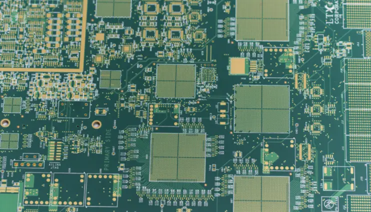
EMC Design Techniques for PCB Layout
Electromagnetic compatibility is usually treated as a test that happens at the end, when the board is finished and the enclosure is closed. By then most of the outcome has already been decided, because emissions and immunity are properties of the layout, and the layout is where they can be controlled cheaply.
Current Returns to Its Source
Every signal current has a return current, and the return takes the path of least impedance. At high frequency that path is directly beneath the trace, in the reference plane, because that is where the loop area is smallest.
This single fact explains most good EMC practice. If the return path is continuous and adjacent, the loop area is small and the board radiates little. If the plane is split, the return must detour around the gap, the loop area grows, and the structure becomes an antenna.
Plane Splits and Their Cost
A plane split is often created for a good reason, such as separating analog and digital grounds. The problem is that a trace crossing that split cannot use the plane beneath it for its return, and the current finds another path, which may be far away.
Where a split is necessary, the rule is that no trace should cross it. If a signal must get from one region to another, it should do so over a continuous plane, with the split handled by a bridge or by placing the crossing carefully. The considerations that drive those splits are covered in our layer assignment article.
<img src="https://www.gopcba.com/wp-content/uploads/2026/08/electronic-components.jpg" alt="PCB layout prepared for EMC testing with a ground plane” />
Loop Area and Component Placement
Any loop carrying a changing current radiates in proportion to its area. The loops that matter most are the ones carrying the largest current at the highest rate of change: switching supplies, clock drivers and any power path with a fast edge.
Keeping those loops small is a placement decision, not a routing one. The input capacitor of a switching regulator belongs beside the regulator, not at the edge of the board, and the return of a clock driver belongs as close to the driver as the signal itself. Placement done well makes the routing easy, and placement done badly cannot be fixed by routing.
Filtering at the Connector
Every cable leaving the board is an antenna. A signal that is quiet on the board can radiate efficiently once it is travelling along a metre of cable, and the connector is where that conversion happens.
Filter components belong at the connector, before the cable, so that the current has to pass through them rather than finding a path around them. A filter placed near the device instead protects the device but does nothing for the cable, which is the opposite of what the emissions problem requires.
Grounding and Shielding
A shield works by intercepting the field and providing a return path for the currents it induces. That means its connections matter more than its thickness, and a shield connected at one point only is largely ineffective above a few megahertz.
Where a board sits in a metal enclosure, the mounting points become the shield connections, and their spacing determines the frequency above which the enclosure is effective. Spacing them regularly and keeping the enclosure seams tight does more than adding material. The same principle applies to board level stitching, which is described in our PCB layout notes.
Clock and Switching Nodes
Clocks are periodic, which means their energy is concentrated at specific frequencies where limits apply. Keeping a clock trace short, keeping it referenced to a continuous plane and avoiding stubs removes the resonances that make a clock radiate.
Switching nodes in a power supply are the other concentrated source. The drain or switch node should have the smallest possible copper area consistent with thermal requirements, because a large pad is a large radiating surface. The trade between thermal copper and radiated area is one of the real design decisions in a power layout.
Pre Compliance Testing
Testing before the formal measurement is far cheaper than discovering a problem afterwards. Near field probes and a spectrum analyser can locate the structure that is radiating long before a chamber is booked.
The most useful preparation is to run the product in all of its modes and to measure each one, because emissions often depend on what the product is doing. A board that passes with the radio off and fails with it on has a different problem from one that fails at idle.
Cable and Connector Practice
The connector is where on-board currents become cable currents, and the practice around it decides much of the measured result. Signal and return pins should be adjacent so that the loop is closed at the connector rather than somewhere in the cable.
Connectors with a metal shell should have that shell bonded to the board ground at multiple points. A shell connected by a single trace is an inductance rather than a screen, and the difference is often the gap between passing and failing a radiated emissions limit. Our prototyping notes cover the checks that catch this before the first build.
Immunity as Well as Emissions
Compatibility works both ways. A board must not radiate excessively, and it must also keep working when an external field is applied or when a transient arrives on a cable.
The mechanisms overlap: a small loop area and a continuous reference plane help both. Where the two requirements need different treatment, immunity usually calls for filtering at the connector and for clamping devices at the interfaces that leave the enclosure. The tolerance and reliability consequences are discussed in our reliability article.
Documenting the EMC Decisions
The choices that matter should be recorded with the design, because they are not visible in the schematic. Where the split is, which connector has a filter, where the stitching vias are and what the shield bonding arrangement is.
A later revision that removes one of those features will not know it was load bearing unless the reason was written down. Our design tolerances notes describe how such constraints are recorded on the fabrication drawing.
Recording the measurement as well as the design matters. A board that passes with a margin of a few decibels is a different proposition from one that passes by twenty, and knowing which one is in hand informs how much latitude a later cost reduction has. Our EMC design techniques notes describe the pre compliance approach that produces that figure.
Where the product will be tested at an external laboratory, the test plan should be agreed in advance, including the modes to be exercised and the arrangement of the cables. Both have a larger effect on the result than most layout details, and both are easier to control when they are decided rather than improvised on the day.
FAQ
Is EMC a layout problem or a filter problem? Mostly a layout problem. Filters handle what cannot be fixed by layout, and both are needed, but no filter compensates for a badly split reference plane.
Does a four layer board need a ground plane? It benefits enormously from one. The plane gives every trace a nearby return path, which is the single largest improvement available to a two or four layer design.
When should EMC be considered? At architecture stage, when the stackup and the connector placement are decided. By the time the layout is complete, most of the options have been spent.


1 Comment
Op Amp PCB Design Techniques
[…] the switching currents while still providing a single reference for the whole board. Our article on EMC design techniques describes the return path reasoning behind that […]