
Common PCB Design Mistakes and How to Avoid Them
The electronics industry moves quickly, and the pressure to release a board early is one of the reasons design errors survive into production. Most of the common PCB design mistakes described here are not subtle. They are the ones that look harmless on a schematic and only become visible when the panel is quoted, the stencil is cut or the first article is inspected. Recognising them before they reach the fabricator is far cheaper than discovering them after the order is placed.
Why mistakes survive to production
A board can be electrically perfect and still be unmanufacturable. The schematic review asks whether the circuit is correct; it does not ask whether the pads match the part, whether the trace can carry the current or whether the via structure can be plated. When a design is reviewed only against the netlist, those questions are never asked, and the first person to notice is the shop. Building a second review that covers physical and process constraints is the single most effective way to catch the errors below.
Mistake one: the wrong land pattern
Most layout tools ship with a library of common parts, complete with schematic symbols and land patterns, but a design almost always needs at least one footprint that has to be drawn by hand. That is where errors enter. If the pad spacing is wrong by even half a millimetre, the part will not solder reliably, and the resulting rework costs far more than the time saved by drawing the footprint quickly. Verify every hand-drawn footprint against the manufacturer data sheet, including pad size, pitch, courtyard and the position of pin one, and check the result against a published pad design standard rather than against a similar part that happened to work before.
Mistake two: overusing blind and buried vias
As products shrink, designers reach for blind via and buried via structures to reduce the board footprint and connect inner layers without passing through the whole panel. The technique works, but a blind via consumes routing space on the layers it crosses and adds process steps, and each additional type of hole increases cost and complexity. A design that uses them everywhere can become expensive to build or impossible to plate within the available aspect ratio. Use them where density genuinely requires them, keep them out of the rest of the board, and confirm the structure against the fabricator capability, as described under blind and buried via stack selection.
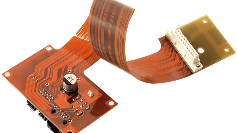
Mistake three: trace width chosen by eye
To keep a board compact, it is tempting to make every trace as narrow as the design rules allow. Trace width is not a single number, though. It depends on the current the net must carry, the permitted temperature rise, the copper weight and whether the trace runs on an inner or an outer layer. A width chosen for a signal net will be inadequate for a supply rail, and a rail that runs warm will drift or fail in the field. Work from the current the net actually carries rather than the minimum the process allows, and use a trace width and current calculation to select the value. For a power net, decide the voltage drop you can tolerate and check the width against it.
Mistake four: skipping the design rule check
A design rule check is only as useful as the rule set behind it. Running the default rules that came with the CAD tool proves nothing about the fabricator’s capability, because the defaults are usually loose. Load the process limits the shop can actually hold, including minimum trace and space, minimum annular ring, drill sizes and via clearance to copper, then run the check and review every remaining violation. Record the accepted exceptions with a reason so the next revision does not have to rediscover them.
Mistake five: forgetting assembly and test
Two reviews that are commonly skipped concern the people who have to build and test the board. Components placed too close together cannot be reworked, and parts placed without regard to the placement order and pad positioning rules may be disturbed by the second soldering step. Equally, a board with no test points cannot be probed, so a single manufacturing defect means scrapping the assembly rather than repairing it. Add rework access, test pads and fiducials to the checklist, and treat them as requirements rather than optional extras.
Mistake six: storing the schematic and the layout as one document
A schematic defines connectivity; a layout defines the physical board. When they are versioned together and edited as though they were the same artefact, a change to one silently invalidates the other. A component added to the schematic but never placed, or a net rerouted on the board but not updated on the drawing, is a defect waiting for the next build. Keep both under independent version control, cross-reference them, and require that a change to either triggers a review of the other.

Building the review that catches them
The remedy is procedural rather than technical. Run a design rule check against the real process capability, then walk three short checklists: one for footprints and pads, one for current, via structure and clearance, and one for assembly and test. Sign off each one. On a dense or high-layer-count board, add a stack-up review with the fabricator before the inner layers are released, because that is the last point at which a change costs nothing. A review that takes an hour at the drawing stage prevents a delay that is measured in weeks.
Mistake seven: ignoring heat and mass in placement
Placement is usually driven by routing convenience, and thermal and mechanical reality is forgotten until the board is in a housing. A regulator that dissipates a watt or more needs copper area and a path into the planes, and a device without that path will run at a temperature the data sheet does not allow. An electrolytic capacitor placed next to a heat source dries out and loses capacitance long before the board fails for any other reason. A heavy component held only by its solder joints will eventually crack them under vibration, so it needs a bracket or adhesive rather than a wider pad. Each of these problems is decided at placement time and cannot be corrected by a process change later. Add a thermal and mechanical check to the same review that covers footprints and clearances, and confirm the copper area under every power device against its dissipation rather than against the size of the pad in the library.
FAQ
What is the most common design error? A hand-drawn land pattern that does not match the part is among the most frequent, because it is invisible on the schematic and only appears at assembly. Verify every manually created footprint against the manufacturer drawing.
Are blind vias a mistake? No, but using them without checking the process is. They solve real density problems and they add real cost, so they belong where the routing genuinely needs them and nowhere else.
Why is a minimum trace width not enough? The minimum is a fabrication limit, not a current rating. A trace sized to the process minimum will overheat if it carries a supply current, so width should be derived from the current and the acceptable temperature rise.